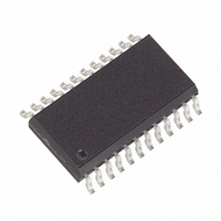
DS17885S-3+ Maxim Integrated Products, DS17885S-3+ Datasheet - Page 24

DS17885S-3+
Manufacturer Part Number
DS17885S-3+
Description
IC RTC 3V 8K NV RAM 24-SOIC
Manufacturer
Maxim Integrated Products
Type
Clock/Calendar/NVSRAMr
Datasheet
1.DS17285S-5.pdf
(31 pages)
Specifications of DS17885S-3+
Memory Size
64K (8K x 8)
Time Format
HH:MM:SS (12/24 hr)
Date Format
YY-MM-DD-dd
Interface
Parallel
Voltage - Supply
2.7 V ~ 3.7 V
Operating Temperature
0°C ~ 70°C
Mounting Type
Surface Mount
Package / Case
24-SOIC (7.5mm Width)
Lead Free Status / RoHS Status
Lead free / RoHS Compliant
At the beginning of interval 3, the system processor has
begun code execution and clears the interrupt condi-
tion of WF and/or KF by writing zeros to both of these
control bits. As long as no other interrupt within the
DS17x85/DS17x87 is pending, the IRQ line is taken
inactive once these bits are reset. Execution of the
application software can proceed. During this time, the
wake-up and kickstart functions can be used to gener-
ate status and interrupts. WF is set in response to a
date, hours, minutes, and seconds match condition. KF
is set in response to a low-going transition on KS. If the
associated interrupt-enable bit is set (WIE and/or KSE),
the IRQ line is driven active low in response to enabled
event. In addition, the other possible interrupt sources
within the DS17885/DS17887 can cause IRQ to be dri-
ven low. While system power is applied, the on-chip
logic always attempts to drive the PWR pin active in
response to the enabled kickstart or wake-up condition.
This is true even if PWR was previously inactive as the
result of power being applied by some means other
than wake-up or kickstart.
The system can be powered down under software con-
trol by setting the PAB bit to logic 1. This causes the
open-drain PWR pin to be placed in a high-impedance
state, as shown at the beginning of interval 4 in the tim-
ing diagram. As V
pin is placed in a high-impedance state when V
goes below V
on in response to a wake-up or kickstart, then the WF
and KF flags should be cleared, and WIE and/or KSE
should be enabled prior to setting the PAB bit.
During interval 5, the system is fully powered down.
Battery backup of the clock calendar and NV RAM is in
effect and IRQ is tri-stated, and monitoring of wake-up
and kickstart takes place. If PRS = 1, PWR stays active;
otherwise, if PRS = 0, PWR is high impedance.
The DS17x85/DS17x87 provide a RAM clear function
for the 114 bytes of user RAM. When enabled, this
function can be performed regardless of the condition
of the V
The RAM clear function is enabled or disabled through
the RAM clear-enable bit (RCE; bank 1, register 04BH).
When this bit is set to logic 1, the 114 bytes of user RAM
is cleared (all bits set to 1) when an active-low transition
is sensed on the RCLR pin. This action has no effect on
either the clock/calendar settings or the contents of the
extended RAM. The RAM clear flag (RF, bank 1, register
04AH) is set when the RAM clear operation has been
Real-Time Clocks
24
____________________________________________________________________
CC
pin.
PF
. If the system is to be again powered
CC
voltage decays, the IRQ output
RAM Clear
CC
completed. If V
clear and RIE = 1, the IRQ line is also driven low upon
completion. Writing a zero to the RF bit clears the inter-
rupt condition. The IRQ line then returns to its inactive
high level, provided there are no other pending inter-
rupts. Once the RCLR pin is activated, all read/write
accesses are locked out for a minimum recover time,
specified as t
When RCE is cleared to 0, the RAM clear function is
disabled. The state of the RCLR pin has no effect on
the contents of the user RAM, and transitions on the
RCLR pin have no effect on RF.
The DS17x85/DS17x87 provide 2k, 4k, or 8k x 8 of on-
chip SRAM that is controlled as nonvolatile storage sus-
tained from a lithium battery. On power-up, the RAM is
taken out of write-protect status by the internal power-
OK signal (POK) generated from the write-protect cir-
cuitry. The on-chip SRAM is accessed through the
eight multiplexed address/data lines AD7 to AD0. Three
on-chip latch registers control access to the SRAM.
Two registers are used to hold the SRAM address, and
the other register is used to hold read/write data.
Access to the extended RAM is controlled by three of
the registers shown in Table 5. The extended registers
in bank 1 must first be selected by setting the DV0 bit
in register A to logic 1. The address of the RAM loca-
tion to be accessed must be loaded into the extended
RAM address registers located at 50h and 51h. The
least significant address byte should be written to loca-
tion 50h, and the most significant bits (right-justified)
should be loaded in location 51h. Data in the
addressed location can be read by performing a read
operation from location 53h, or written to by performing
a write operation to location 53h. Data in any
addressed location can be read or written repeatedly
without changing the address in location 50h and 51h.
To read or write consecutive extended RAM locations,
a burst mode feature can be enabled to increment the
extended RAM address. To enable the burst mode fea-
ture, set the BME bit in the Extended Control Register
4Ah to logic 1. With burst mode enabled, write the
extended RAM starting address location to registers
50h and 51h. Then read or write the extended RAM
data from/to register 53h. The extended RAM address
locations are automatically incremented on the rising
edge of RD or WR only when register 53h is being
accessed. See the Burst Mode Timing Waveform.
REC
CC
in Electrical Characteristics .
is present at the time of the RAM
Extended RAM


