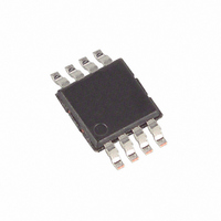
DS1340U-3 Maxim Integrated Products, DS1340U-3 Datasheet - Page 2

DS1340U-3
Manufacturer Part Number
DS1340U-3
Description
IC RTC I2C W/CHARGER 3V 8-USOP
Manufacturer
Maxim Integrated Products
Type
Clock/Calendar/Trickle-Chargerr
Datasheet
1.DS1340U-18.pdf
(16 pages)
Specifications of DS1340U-3
Time Format
HH:MM:SS (24 hr)
Date Format
YY-MM-DD-dd
Interface
I²C, 2-Wire Serial
Voltage - Supply
2.7 V ~ 3.3 V
Operating Temperature
-40°C ~ 85°C
Mounting Type
Surface Mount
Package / Case
8-MSOP, Micro8™, 8-uMAX, 8-uSOP,
Lead Free Status / RoHS Status
Contains lead / RoHS non-compliant
Memory Size
-
Available stocks
Company
Part Number
Manufacturer
Quantity
Price
Part Number:
DS1340U-3+T
Manufacturer:
MAXIM/美信
Quantity:
20 000
Part Number:
DS1340U-33
Manufacturer:
MAXIM/美信
Quantity:
20 000
Company:
Part Number:
DS1340U-33+
Manufacturer:
PARADE
Quantity:
1 183
Part Number:
DS1340U-33+T
Manufacturer:
MAXIM/美信
Quantity:
20 000
Part Number:
DS1340U-33+T&R
Manufacturer:
MAXIM/美信
Quantity:
20 000
Company:
Part Number:
DS1340U-33+TR
Manufacturer:
NEC
Quantity:
351
ABSOLUTE MAXIMUM RATINGS
Voltage Range on V
Voltage Range on SDA, SCL, and FT/OUT
Operating Temperature Range ...........................-40°C to +85°C
I
AC ELECTRICAL CHARACTERISTICS
(V
Stresses beyond those listed under “Absolute Maximum Ratings” may cause permanent damage to the device. These are stress ratings only, and functional
operation of the device at these or any other conditions beyond those indicated in the operational sections of the specifications is not implied. Exposure to
absolute maximum rating conditions for extended periods may affect device reliability.
2
SCL Clock Frequency
Bus Free Time Between STOP
and START Conditions
Hold Time (Repeated) START
Condition (Note 2)
Low Period of SCL Clock
High Period of SCL Clock
Data Hold Time (Notes 3, 4)
Data Setup Time (Note 5)
START Setup Time
Rise Time of SDA and SCL
Signals (Note 6)
Fall Time of SDA and SCL Signals
(Note 6)
Setup Time for STOP Condition
Capacitive Load for Each Bus
Line
I/O Capacitance (SCL, SDA)
Pulse Width of Spikes that Must
be Suppressed by the Input Filter
Oscillator Stop Flag (OSF) Delay
2
CC
Relative to Ground..................................-0.3V to (V
C RTC with Trickle Charger
_____________________________________________________________________
= V
CC MIN
PARAMETER
to V
CC
CC MAX
Pin Relative to Ground .....-0.3V to +6.0V
, T
A
= -40°C to +85°C, unless otherwise noted.) (Note 1, Figure 1)
SYMBOL
t
t
t
t
t
HD:DAT
HD:STA
SU:DAT
SU:STA
SU:STO
t
t
f
t
HIGH
C
t
LOW
SCL
BUF
C
t
OSF
t
t
SP
I/O
R
F
B
Standard mode
Fast mode
Standard mode
Fast mode
Standard mode
Fast mode
Standard mode
Fast mode
Standard mode
Fast mode
Standard mode
Fast mode
Standard mode
Fast mode
Standard mode
Fast mode
Standard mode
Fast mode
Standard mode
Fast mode
Standard mode
Fast mode
(Note 6)
Fast mode
(Note 7)
CC
+ 0.3V)
CONDITIONS
Storage Temperature Range .............................-55°C to +125°C
Lead Temperature (soldering, 10s) .................................+260°C
Soldering Temperature (reflow) .......................................+260°C
20 + 0.1C
20 + 0.1C
20 + 0.1C
20 + 0.1C
MIN
100
250
100
4.7
1.3
4.0
0.6
4.7
1.3
4.0
0.6
4.7
0.6
4.7
0.6
0
0
0
B
B
B
B
TYP
100
10
30
MAX
1000
100
400
300
300
300
400
0.9
0.9
UNITS
kHz
ms
pF
pF
µs
µs
µs
µs
µs
ns
µs
ns
ns
µs
ns


