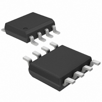
DS1672S-3+ Maxim Integrated Products, DS1672S-3+ Datasheet - Page 10

DS1672S-3+
Manufacturer Part Number
DS1672S-3+
Description
IC TIMEKEEPER 3V 32-BIT 8-SOIC
Manufacturer
Maxim Integrated Products
Type
Clock/Calendar/Trickle-Chargerr
Datasheet
1.DS1672S-33.pdf
(15 pages)
Specifications of DS1672S-3+
Time Format
Binary
Date Format
Binary
Interface
I²C, 2-Wire Serial
Voltage - Supply
2.7 V ~ 3.3 V
Operating Temperature
-40°C ~ 85°C
Mounting Type
Surface Mount
Package / Case
8-SOIC (3.9mm Width)
Lead Free Status / RoHS Status
Lead free / RoHS Compliant
Memory Size
-
Microprocessor Monitor
A temperature-compensated comparator circuit monitors the level of V
fail trip point, the RST signal (open drain) is pulled active and read/write access is inhibited. When V
returns to nominal levels, the RST signal is kept in the active state for t
supply and microprocessor to stabilize. Note, however, that if the EOSC bit is set to a logic 1 (to disable
the oscillator during write protection), the reset signal will be kept in an active state for t
startup time of the oscillator.
Trickle Charger
The trickle charger is controlled by the trickle charge register. The simplified schematic of Figure 5
shows the basic components of the trickle charger. The trickle charge select (TCS) bit (bits 4–7) controls
the selection of the trickle charger. In order to prevent accidental enabling, only a pattern on 1010 will
enable the trickle charger. All other patterns will disable the trickle charger. The DS1672 powers up with
the trickle charger disabled. The diode select (DS) bits (bits 2, 3) select whether or not a diode is
connected between V
The RS bits (bits 0, 1) select whether a resistor is connected between V
of the resistor is. The resistor selected by the resistor select (RS) bits and the diode selected by the diode
select (DS) bits are as follows:
Diode and resistor selection is determined by the user according to the maximum current desired for
battery or super cap charging. The maximum charging current can be calculated as illustrated in the
following example. Assume that a system power supply of 3V is applied to V
connected to V
between V
As the super cap changes, the voltage drop between V
charge current will decrease.
TCS
X
X
X
1
1
1
1
1
1
0
TCS
X
X
X
0
0
0
0
0
0
0
CC
and V
BACKUP
TCS
X
X
X
1
1
1
1
1
1
0
BACKUP
I
CC
MAX
. Also assume that the trickle charger has been enabled with a diode and resistor R2
TCS
and V
X
X
X
0
0
0
0
0
0
0
= (5.0V - diode drop) / R1 (5.0V - 0.7V) / 2k 2.2mA
. The maximum current I
BACKUP
DS
X
0
1
0
1
0
1
0
0
1
. If DS is 01, no diode is selected or if DS is 10, a diode is selected.
DS
X
0
1
1
0
1
0
1
0
0
RS
X
X
0
0
1
1
1
1
0
0
10 of 15
MAX
CC
RS
X
X
would, therefore, be calculated as follows:
0
1
1
0
0
1
1
0
and V
Disabled
Disabled
Disabled
No diode, 250 resistor
One diode, 250 resistor
No diode, 2k resistor
One diode, 2k resistor
No diode, 4k resistor
One diode, 4k resistor
Initial default value—disabled
BACKUP
will decrease and, therefore, the
CC
FUNCTION
RPU
CC
and V
. When V
(typically) to allow the power
CC
BACKUP
and a super cap is
CC
falls to the power-
and what the value
RPU
plus the
CC


