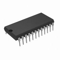
DS12CR887-5+ Maxim Integrated Products, DS12CR887-5+ Datasheet - Page 10

DS12CR887-5+
Manufacturer Part Number
DS12CR887-5+
Description
IC RTC W/RAM 128 BYTE 24-EDIP
Manufacturer
Maxim Integrated Products
Type
Clock/Calendar/NVSRAMr
Datasheet
1.DS12R885S-33.pdf
(23 pages)
Specifications of DS12CR887-5+
Memory Size
114B
Time Format
HH:MM:SS (12/24 hr)
Date Format
YY-MM-DD-dd
Interface
Parallel
Voltage - Supply
4.5 V ~ 5.5 V
Operating Temperature
-40°C ~ 85°C
Mounting Type
Through Hole
Package / Case
24-DIP (600 mil) Module
Function
Clock/Calendar
Rtc Memory Size
114 Byte
Supply Voltage (max)
5.5 V
Supply Voltage (min)
4.5 V
Maximum Operating Temperature
+ 85 C
Minimum Operating Temperature
- 40 C
Mounting Style
Through Hole
Rtc Bus Interface
Multiplexed
Lead Free Status / RoHS Status
Lead free / RoHS Compliant
RTCs with Constant-Voltage Trickle Charger
10
12, 16
SO
13
14
15
22
17
____________________________________________________________________
2, 3, 16,
20–22
EDIP
PIN
12
13
14
15
17
D5–D8,
E1–E8,
F5–F8
BGA
C1
C3
C2
A3
A1
NAME
GND
N.C.
R/W
CS
AS
DS
Ground
Chip-Select Input. The active-low chip-select signal must be asserted low for a bus cycle
in the DS12R885 to be accessed. CS must be kept in the active state during DS and AS
for Motorola timing and during DS and R/W for Intel timing. Bus cycles that take place
without asserting CS latch addresses, but no access occurs. When V
the DS12R885 inhibits access by internally disabling the CS input. This action protects the
RTC data and the RAM data during power outages.
Address Strobe Input. A positive-going address-strobe pulse serves to demultiplex the
bus. The falling edge of AS causes the address to be latched within the DS12R885. The
next rising edge that occurs on the AS bus clears the address regardless of whether CS is
asserted. An address strobe must immediately precede each write or read access. If a
write or read is performed with CS deasserted, another address strobe must be performed
prior to a read or write access with CS asserted.
Read/Write Input. The R/W pin has two modes of operation. When the MOT pin is
connected to V
cycle is a read or write. A read cycle is indicated with a high level on R/W while DS is high.
A write cycle is indicated when R/W is low during DS. When the MOT pin is connected to
GND for Intel timing, the R/W signal is an active-low signal. In this mode, the R/W pin
operates in a similar fashion as the write-enable signal (WE) on generic RAMs. Data are
latched on the rising edge of the signal.
No Connection. This pin should remain unconnected. On the EDIP, these pins are missing
by design.
Data Strobe or Read Input. The DS pin has two modes of operation depending on the level of
the MOT pin. When the MOT pin is connected to V
mode, DS is a positive pulse during the latter portion of the bus cycle and is called data
strobe. During read cycles, DS signifies the time that the DS12R885 is to drive the
bidirectional bus. In write cycles, the trailing edge of DS causes the DS12R885 to latch the
written data. When the MOT pin is connected to GND, Intel bus timing is selected. DS
identifies the time period when the DS12R885 drives the bus with read data. In this mode, the
DS pin operates in a similar fashion as the output-enable (OE) signal on a generic RAM.
CC
for Motorola timing, R/W is at a level that indicates whether the current
FUNCTION
Pin Description (continued)
CC
, Motorola bus timing is selected. In this
CC
is below V
PF
volts,


