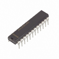
DS17887-5 Maxim Integrated Products, DS17887-5 Datasheet - Page 18

DS17887-5
Manufacturer Part Number
DS17887-5
Description
IC RTC 5V 8K NV RAM 24-EDIP
Manufacturer
Maxim Integrated Products
Type
Clock/Calendar/NVSRAMr
Datasheet
1.DS17285S-5.pdf
(31 pages)
Specifications of DS17887-5
Memory Size
64K (8K x 8)
Time Format
HH:MM:SS (12/24 hr)
Date Format
YY-MM-DD-dd
Interface
Parallel
Voltage - Supply
4.5 V ~ 5.5 V
Operating Temperature
0°C ~ 70°C
Mounting Type
Through Hole
Package / Case
24-DIP (600 mil) Module
Lead Free Status / RoHS Status
Contains lead / RoHS non-compliant
Other names
DS178875
Available stocks
Company
Part Number
Manufacturer
Quantity
Price
Company:
Part Number:
DS17887-5
Manufacturer:
DALLAS
Quantity:
94
Company:
Part Number:
DS17887-5
Manufacturer:
MOLEX
Quantity:
140
Part Number:
DS17887-5
Manufacturer:
DALLAS
Quantity:
20 000
Part Number:
DS17887-5+
Manufacturer:
DALLAS
Quantity:
20 000
Company:
Part Number:
DS17887-5+IND
Manufacturer:
AMP
Quantity:
472
The user RAM bytes are not dedicated to any special
function within the DS17x85. They can be used by the
processor program as battery-backed memory and are
fully available during the update cycle.
The user RAM is divided into two separate memory
banks. When the bank 0 is selected, the 14 real-time
clock registers and 114 bytes of user RAM are accessi-
ble. When bank 1 is selected, an additional 2kbytes,
4kbytes, or 8kbytes of user RAM are accessible
through the extended RAM address and data registers.
The RTC includes six separate, fully automatic sources
of interrupt for a processor:
The conditions that generate each of these indepen-
dent interrupt conditions are described in detail in other
sections of this data sheet. This section describes the
overall control of the interrupts.
The application software can select which interrupts, if
any, are to be used. There are 6 bits, including 3 bits in
Register B and 3 bits in Extended Register 4B, that
enable the interrupts. The extended register locations
are described later. Writing logic 1 to an interrupt-
enable bit permits that interrupt to be initiated when the
event occurs. A logic 0 in the interrupt-enable bit pro-
hibits the IRQ pin from being asserted from that interrupt
condition. If an interrupt flag is already set when an
interrupt is enabled, IRQ is immediately set at an active
level, although the event initiating the interrupt condition
might have occurred much earlier. Therefore, there are
cases where the software should clear these earlier
generated interrupts before first enabling new interrupts.
When an interrupt event occurs, the relating flag bit is
set to logic 1 in Register C or in Extended Register 4A.
These flag bits are set regardless of the setting of the
corresponding enable bit located either in Register B or
in Extended Register 4B. The flag bits can be used in a
polling mode without enabling the corresponding
enable bits.
However, care should be taken when using the flag bits
of Register C as they are automatically cleared to 0
immediately after they are read. Double latching is
Real-Time Clocks
18
1) Alarm Interrupt
2) Periodic Interrupt
3) Update-Ended Interrupt
4) Wake-Up Interrupt
5) Kickstart Interrupt
6) RAM Clear Interrupt
____________________________________________________________________
Nonvolatile RAM
Interrupts
implemented on these bits so that set bits remain sta-
ble throughout the read cycle. All bits that were set are
cleared when read and new interrupts that are pending
during the read cycle are held until after the cycle is
completed. One, two, or three bits can be set when
reading Register C. Each used flag bit should be exam-
ined when read to ensure that no interrupts are lost.
The flag bits in Extended Register 4A are not automati-
cally cleared following a read. Instead, each flag bit
can be cleared to 0 only by writing 0 to that bit.
When using the flag bits with fully enabled interrupts,
the IRQ line is driven low when an interrupt flag bit is
set and its corresponding enable bit is also set. IRQ is
held low as long as at least one of the six possible
interrupt sources has its flag and enable bits both set.
The IRQF bit in Register C is 1 whenever the IRQ pin is
being driven low as a result of one of the six possible
active sources. Therefore, determination that the
DS17x85/DS17x87 initiated an interrupt is accom-
plished by reading Register C and finding IRQF = 1.
IRQF remains set until all enabled interrupt flag bits are
cleared to 0.
A pattern of 01X in bits 4 to 6 of Register A turns the
oscillator on and enables the countdown chain. A pat-
tern of 11X (DV2 = 1, DV1 = 1, DV0 = X) turns the oscil-
lator on, but holds the countdown chain of the oscillator
in reset. All other combinations of bits 4 to 6 keep the
oscillator off.
When the DS17x87 is shipped from the factory, the
internal oscillator is turned off. This feature prevents the
lithium energy cell from being used until it is installed in
a system.
Thirteen of the 15 divider taps are made available to a
1-of-16 multiplexer, as shown in Figure 1. The square
wave and periodic interrupt generators share the out-
put of the multiplexer. The RS0–RS3 bits in Register A
establish the output frequency of the multiplexer. These
frequencies are listed in Table 4. Once the frequency is
selected, the output of the SQW pin can be turned on
and off under program control with the square-wave
enable bit (SQWE).
If E32K = 0, the square-wave output is determined by
the RS3 to RS0 bits. If E32K = 1, a 32kHz square wave
is output on the SQW pin, regardless of the RS3 to RS0
bits’ state. If E32K = ABE = 1 and a valid voltage is
applied to V
SQW when V
Square-Wave Output Selection
BAUX
CC
is below V
, a 32kHz square wave is output on
Oscillator Control Bits
TP
.


