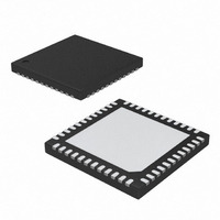
MAX5865ETM+T Maxim Integrated Products, MAX5865ETM+T Datasheet - Page 15

MAX5865ETM+T
Manufacturer Part Number
MAX5865ETM+T
Description
IC ANLG FRONT END 40MSPS 48-TQFN
Manufacturer
Maxim Integrated Products
Datasheet
1.MAX5865ETM.pdf
(26 pages)
Specifications of MAX5865ETM+T
Number Of Bits
10
Number Of Channels
4
Power (watts)
2.10W
Voltage - Supply, Analog
2.7 V ~ 3.3 V
Voltage - Supply, Digital
1.8 V ~ 3.3 V
Package / Case
48-TQFN Exposed Pad
Lead Free Status / RoHS Status
Lead free / RoHS Compliant
Figure 3
log inputs, and the resulting output data. Channel IA
(CHI) and channel QA (CHQ) are simultaneously sam-
pled on the rising edge of the clock signal (CLK) and
the resulting data is multiplexed at the DA0–DA7 out-
Figure 2. ADC Transfer Function
Figure 3. ADC System Timing Diagram
DA0–DA7
CHQ
CLK
CHI
t
1111 1111
1111 1110
1111 1101
1000 0001
1000 0000
0111 1111
0000 0011
0000 0010
0000 0001
0000 0000
DOQ
shows the relationship between the clock, ana-
-128
D0Q
-127
1 LSB =
______________________________________________________________________________________
-126 -125
ADC System Timing Requirements
Performance, 40Msps Analog Front End
2 x V
V
D1I
256
REF
REF
INPUT VOLTAGE (LSB)
t
DOI
D1Q
-1
(COM)
0
+1
5 CLOCK-CYCLE LATENCY (CHI), 5.5 CLOCK-CYCLE LATENCY (CHQ)
V
REF
D2I
Ultra-Low-Power, High-Dynamic-
V
= V
REF
REFP
+125
- V
+126
D2Q
REFN
+127
+128
(COM)
D3I
D3Q
puts. CHI data is updated on the rising edge and CHQ
data is updated on the falling edge of the CLK.
Including the delay through the output latch, the total
clock-cycle latency is 5 clock cycles for CHI and 5.5
clock cycles for CHQ.
The 10-bit DACs are capable of operating with clock
speeds up to 40MHz. The DAC’s digital inputs,
DD0–DD9, are multiplexed on a single 10-bit bus. The
voltage reference determines the data converters’ full-
scale output voltages. See the Reference Configurations
section for setting reference voltage. The DACs utilize a
current-array technique with a 1mA (with 1.024V refer-
ence) full-scale output current driving a 400Ω internal
resistor resulting in a ±400mV full-scale differential out-
put voltage. The MAX5865 is designed for differential
output only and is not intended for single-ended appli-
cation. The analog outputs are biased at 1.4V common
mode and designed to drive a differential input stage
with input impedance ≥70kΩ. This simplifies the analog
interface between RF quadrature upconverters and the
MAX5865. RF upconverters require a 1.3V to 1.5V com-
mon-mode bias. The internal DC common-mode bias
eliminates discrete level setting resistors and code-gen-
erated level-shifting while preserving the full dynamic
range of each transmit DAC.
voltage vs. input code.
D4I
D4Q
D5I
Table 2
D5Q
Dual 10-Bit DAC
D6I
shows the output
D6Q
15


