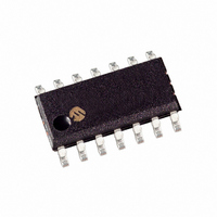
MCP3302-BI/SL Microchip Technology, MCP3302-BI/SL Datasheet - Page 19

MCP3302-BI/SL
Manufacturer Part Number
MCP3302-BI/SL
Description
IC ADC 13BIT 2.7V 2CH SPI 14SOIC
Manufacturer
Microchip Technology
Datasheet
1.MCP3302-CIST.pdf
(46 pages)
Specifications of MCP3302-BI/SL
Number Of Bits
13
Sampling Rate (per Second)
100k
Data Interface
Serial, SPI™
Number Of Converters
1
Voltage Supply Source
Single Supply
Operating Temperature
-40°C ~ 85°C
Mounting Type
Surface Mount
Package / Case
14-SOIC (0.154", 3.90mm Width)
Lead Free Status / RoHS Status
Lead free / RoHS Compliant
Other names
MCP3302BI/SL
Available stocks
Company
Part Number
Manufacturer
Quantity
Price
Company:
Part Number:
MCP3302-BI/SL
Manufacturer:
MICROCHIP
Quantity:
12 000
Part Number:
MCP3302-BI/SL
Manufacturer:
MICROCHI
Quantity:
20 000
5.0
5.1
The
conventional SAR architecture. With this architecture,
the potential between the IN+ and IN- inputs are
simultaneously sampled and stored with the internal
sample circuits for 1.5 clock cycles. Following this
sampling time, the input hold switches of the converter
open and the device uses the collected charge to
produce a serial 13-bit binary two’s complement output
code. This conversion process is driven by the external
clock and must include 13 clock cycles, one for each
bit. During this process, the most significant bit (MSB)
is output first. This bit is the sign bit and indicates if the
IN+ or IN- input is at a higher potential.
FIGURE 5-1:
© 2008 Microchip Technology Inc.
IN+
IN-
MCP3302/04
Hold
Hold
APPLICATIONS INFORMATION
Conversion Description
C
C
SAMP
SAMP
Simplified Block Diagram.
A/D
+
-
converters
Comp
CDAC
D
13-Bit SAR
OUT
Register
employ
Shift
a
5.2
The analog input of the MCP3302/04 is easily driven,
either differentially or single ended. Any signal that is
common to the two input channels will be rejected by
the common mode rejection of the device. During the
charging time of the sample capacitor, a small charging
current will be required. For low-source impedances,
this input can be driven directly. For larger source
impedances, a larger acquisition time will be required
due to the RC time constant that includes the source
impedance.
specification, the charge holding capacitor (C
must be given enough time to acquire a 13-bit accurate
voltage level during the 1.5 clock cycle acquisition
period.
An analog input model is shown in
model is accurate for an analog input, regardless if it is
configured as a single ended input, or the IN+ and IN-
input in differential mode. In this diagram, it is shown
that the source impedance (R
sampling switch (R
time that is required to charge the capacitor (C
Consequently, a larger source impedance with no
additional acquisition time increases the offset, gain
and integral linearity errors of the conversion. To
overcome this, a slower clock speed can be used to
allow for the longer charging time.
the maximum clock speed associated with source
impedances.
FIGURE 5-2:
vs. Source Resistance (R
INL.
2.5
2.0
1.5
1.0
0.5
0.0
100
Driving the Analog Input
For
SS
Source Resistance (ohms)
the
1000
) impedance, directly affecting the
MCP3302/04
Maximum Clock Frequency
A/D
S
) to maintain ±1 LSB
S
) adds to the internal
Converter
10000
DS21697E-page 19
Figure 5-2
Figure
to
5-3. This
SAMPLE
SAMPLE
100000
shows
meet
).
)


