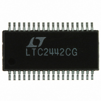
LTC2442CG#PBF Linear Technology, LTC2442CG#PBF Datasheet - Page 7

LTC2442CG#PBF
Manufacturer Part Number
LTC2442CG#PBF
Description
IC ADC 24BIT 4CH 36-SSOP
Manufacturer
Linear Technology
Datasheet
1.LTC2442CGPBF.pdf
(32 pages)
Specifications of LTC2442CG#PBF
Number Of Bits
24
Sampling Rate (per Second)
8k
Data Interface
MICROWIRE™, Serial, SPI™
Number Of Converters
1
Power Dissipation (max)
50mW
Voltage Supply Source
Single Supply
Operating Temperature
0°C ~ 70°C
Mounting Type
Surface Mount
Package / Case
36-SSOP (0.200", 5.30mm Width)
Lead Free Status / RoHS Status
Lead free / RoHS Compliant
Available stocks
Company
Part Number
Manufacturer
Quantity
Price
PI FU CTIO S
SCK (Pin 1): Bidirectional Digital Clock Pin. In internal serial
clock operation mode, SCK is used as a digital output for
the internal serial interface clock during the data output
period. In the external serial clock operation mode, SCK
is used as the digital input for the external serial interface
clock during the data output period. The serial clock op-
eration mode is determined by the logic level applied to
EXT (Pin 3).
BUSY (Pin 2): Conversion in Progress Indicator. This pin
is HIGH while the conversion is in progress and goes LOW
indicating the conversion is complete and data is ready.
It remains LOW during the sleep and data output states.
At the conclusion of the data output state, it goes HIGH
indicating a new conversion has begun.
EXT (Pin 3): Internal/External SCK Selection Pin. This
pin is used to select internal or external SCK for output-
ting/inputting data. If EXT is tied low, the device is in the
external SCK mode and data is shifted out of the device
under the control of a user applied serial clock. If EXT is
tied high, the internal serial clock mode is selected. The
device generates its own SCK signal and outputs this on
the SCK pin. A framing signal BUSY (Pin 2) goes low
indicating data is being output.
GND (Pins 4, 5, 32): Ground. Multiple ground pins inter-
nally connected for optimum ground current fl ow and V
decoupling. Connect each one of these pins to a common
ground plane through a low impedance connection. All three
pins must be connected to ground for proper operation.
CH0 to CH3 (Pins 6, 7, 8, 9): Analog Inputs. May be
programmed for single-ended or differential mode. (See
Table 3)
ANCINB (Pin 10): ADC Input. Must tie to the amplifi er
output, OUTB (Pin 17).
U
U
U
CC
ADCINA (Pin 11): ADC Input. Must tie to the amplifi er
output, OUTA (Pin 12).
OUTA (Pin 12): Amplifi er A output. Must be compensated
with 0.1µF or greater capacitor. Drives the ADCINA ADC
input (Pin 11).
–INA (Pin 13): Amplifi er A negative Input. By shorting this
pin to OUTA (Pin 12) the amplifi er becomes a buffer with
unity gain. Alternatively, an external resistor network may
be added here for gains greater than 1.
NC (Pins 14, 15, 16, 20, 22, 23): No Connect. These pins
should be left fl oating or tied to Ground.
OUTB (Pin 17): Amplifi er B Output. Must be compensated
with 0.1µF or greater capacitor. Drives the ADCINB ADC
input (Pin 10).
–INB (Pin 18): Amplifi er B negative Input. By shorting this
pin to OUTB (Pin 17) the amplifi er becomes a buffer with
unity gain. Alternatively, an external resistor network may
be added here for gains greater than 1.
+INB (Pin 19): Amplifi er B positive Input. Must tie to the
Multiplexer output MUXOUTB (Pin 26).
V
tie to V
to GND with 1µF capacitor.
V
tie to GND or an external supply voltage as low as –15V.
Bypass to GND with a 1µF capacitor.
+INA (Pin 25): Amplifi er A positive Input. Must tie to the
Multiplexer output MUXOUTA (Pin 27).
MUXOUTB (Pin 26): Multiplexer Output. Must tie to +INB
amplifi er input (Pin 19).
+
–
(Pin 24): Amplifi er Negative supply voltage input. May
(Pin 21): Amplifi er positive supply voltage input. May
CC
or an external supply voltage up to 15V. Bypass
LTC2442
7
2442f


