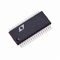
LTC1608CG#PBF Linear Technology, LTC1608CG#PBF Datasheet

LTC1608CG#PBF
Specifications of LTC1608CG#PBF
Available stocks
Related parts for LTC1608CG#PBF
LTC1608CG#PBF Summary of contents
Page 1
... The ADC has P compatible,16-bit parallel output port. There is no pipeline delay in conversion results. A separate convert start input and a data ready signal (BUSY) ease connections to FlFOs, DSPs and microprocessors. , LTC and LT are registered trademarks of Linear Technology Corporation. Circuitry in the LTC1608 is covered under US Patent #5,764,175 ...
Page 2
LTC1608 ABSOLUTE AXI U RATI (Notes Supply Voltage (V ) ................................................ 6V DD Negative Supply Voltage (V ) ............................... – Total ...
Page 3
ACCURACY SYMBOL PARAMETER S/N Signal-to-Noise Ratio S/( Signal-to-(Noise + Distortion) Ratio THD Total Harmonic Distortion Up to 5th Harmonic SFDR Spurious Free Dynamic Range IMD Intermodulation Distortion Full Power Bandwidth Full Linear Bandwidth ...
Page 4
LTC1608 W U POWER REQUIRE E TS otherwise specifications are (Note 5) A SYMBOL PARAMETER V Positive Supply Voltage DD V Negative Supply Voltage SS I Positive Supply Current DD Nap Mode Sleep Mode I ...
Page 5
ELECTRICAL CHARACTERISTICS Note 4: When these pin voltages are taken below V by internal diodes. This product can handle input currents greater than 100mA below V without latchup. These pins are not clamped Note ...
Page 6
LTC1608 W U TYPICAL PERFOR A CE CHARACTERISTICS Intermodulation Distortion 500kHz SAMPLE f = 96.56kHz IN1 – 99.98kHz IN2 –40 –60 –80 –100 –120 –140 0 50 100 150 200 250 FREQUENCY (kHz) 1608 G07 ...
Page 7
CTIO AL BLOCK DIAGRA REFCOMP DIFFERENTIAL ANALOG INPUT 2 A 2.5V IN TEST CIRCUITS Load Circuits for Access Timing (A) Hi AND V ...
Page 8
LTC1608 U U APPLICATIO S I FOR ATIO C SMPL SAMPLE + A IN HOLD ZEROING SWITCHES C SMPL SAMPLE – HOLD +C DAC –C DAC +V DAC –V DAC SAR Figure 1. Simplified Block Diagram compared with ...
Page 9
U U APPLICATIO S I FOR ATIO CONVST Figure 3. CS top CONVST Setup Timing CONV 250 500 750 1000 CONVST LOW TIME, t Figure 4. Change ...
Page 10
LTC1608 U U APPLICATIO S I FOR ATIO CONVST t 6 BUSY DATA (N – 1) DATA D15 TO D0 Figure 5. Mode 1a. CONVST Starts a Conversion. Data Outputs Always Enabled (CONVST ...
Page 11
U U APPLICATIO S I FOR ATIO CONVST t 6 BUSY t 10 DATA CONVST t 6 BUSY DATA spike while charging the sample-and-hold capacitors at the end of conversion. ...
Page 12
... DC accuracy and settling time are most critical. The following list is a summary of the op amps that are suitable for driving the LTC1608. More detailed informa- tion is available in the Linear Technology databooks, the TM LinearView CD-ROM and on our web site at: www.linear-tech. com. ® ...
Page 13
U U APPLICATIO S I FOR ATIO V 3 REF 2.500V REFCOMP 4 REFERENCE 4.375V AMP 12k R3 16k AGND 5 Figure 12a. LTC1608 Reference Circuit 5V 1 ANALOG INPUT LT1019A-2 OUT ...
Page 14
LTC1608 U U APPLICATIO S I FOR ATIO Differential inputs allow greater flexibility for accepting different input ranges. Figure 14b shows a circuit that converts analog input signal with only an additional buffer that is not ...
Page 15
U U APPLICATIO S I FOR ATIO applications where the ADC data outputs and control signals are connected to a continuously active micropro- cessor bus possible to get errors in the conversion results. These errors are due to ...
Page 16
LTC1608 U U APPLICATIO S I FOR ATIO JP1 C13 C12 LTC1608 V REF DD1 C11 ...
Page 17
U U APPLICATIO S I FOR ATIO Figure 17b. Suggested Evaluation Circuit Board. Component Side Silkscreen and Signal Traces ANALOG GROUND PLANE Figure 17d. Suggested Evaluation Circuit Board. Inner Layer 1 Showing Separate Analog and Digital Ground Planes 2500 2000 ...
Page 18
LTC1608 U U APPLICATIO S I FOR ATIO 0 f SAMPLE f = 2.807kHz IN –20 SINAD = 88.9dB THD = –98dB –40 –60 –80 –100 –120 –140 50 100 150 0 FREQUENCY (kHz) Figure 19a. This FFT of the ...
Page 19
... FLASH SHALL NOT EXCEED .254mm (.010") PER SIDE Information furnished by Linear Technology Corporation is believed to be accurate and reliable. However, no responsibility is assumed for its use. Linear Technology Corporation makes no represen- tation that the interconnection of its circuits as described herein will not infringe on existing patent rights. ...
Page 20
... Low Power, Low Gritch, 4-Quadrant Multiplication DGND DD DD SHDN LTC1608 CONTROL LOGIC CONVST 31 CONTROL AND 2. LINES TIMING REF BUSY OGND 28 OUTPUT B15 TO B0 16-BIT BUFFERS D15 TO D0 PARALLEL BUS AGND –5V 1608fs, sn1608 LT/TP 0601 2K • PRINTED IN USA LINEAR TECHNOLOGY CORPORATION 2000 1608 TA03 ...


