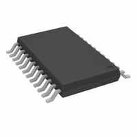
AD7191BRUZ Analog Devices Inc, AD7191BRUZ Datasheet

AD7191BRUZ
Specifications of AD7191BRUZ
Available stocks
Related parts for AD7191BRUZ
AD7191BRUZ Summary of contents
Page 1
FEATURES Pin-programmable output rate Output data rate: 10 Hz, 50 Hz, 60 Hz, 120 Hz Pin-programmable PGA Gain 64, 128 Pin-programmable power-down and reset RMS noise (gain = 128 21.5 noise ...
Page 2
AD7191 TABLE OF CONTENTS Features .............................................................................................. 1 Interface ............................................................................................. 1 Applications ....................................................................................... 1 General Description ......................................................................... 1 Functional Block Diagram .............................................................. 1 Revision History ............................................................................... 2 Specifications ..................................................................................... 3 Timing Characteristics ................................................................ 6 Timing Diagram ........................................................................... 6 Absolute Maximum Ratings ...
Page 3
SPECIFICATIONS 5. 2 5.25 V; AGND = DGND = 0 V; REFIN(+) = specifications unless otherwise noted. MIN MAX Table 1. 1 Parameter ...
Page 4
AD7191 1 Parameter Analog Input Current 2 Input Current Input Current Drift REFERENCE INPUT REFIN Voltage 2 Reference Voltage Range 2 Absolute REFIN Voltage Limits Average Reference Input Current Average Reference Input Current Drift 2 Normal-Mode Rejection Common-Mode Rejection TEMPERATURE ...
Page 5
Parameter Floating-State Leakage Current Floating-State Output Capacitance Data Output Coding 3 POWER REQUIREMENTS Power Supply Voltage AV − AGND DD DV − DGND DD Power Supply Currents AI Current DD DI Current DD I (Power-Down Mode Temperature ...
Page 6
AD7191 TIMING CHARACTERISTICS 5. 2 5.25 V; AGND = DGND = 0 V, Input Logic Input Logic Table ...
Page 7
ABSOLUTE MAXIMUM RATINGS T = 25°C, unless otherwise noted. A Table 3. Parameter AV to AGND DGND DD AGND to DGND Analog Input Voltage to AGND Reference Input Voltage to AGND Digital Input Voltage to DGND Digital ...
Page 8
AD7191 PIN CONFIGURATION AND FUNCTION DESCRIPTIONS Table 4. Pin Function Descriptions Pin No. Mnemonic Description When the master clock for the device is provided externally by a crystal, the crystal is connected between 1 MCLK1 MCLK1 and MCLK2. Alternatively, the ...
Page 9
Pin No. Mnemonic Description 20 AV Analog Supply Voltage 5. with Digital Supply Voltage with DV 22 ODR1 Output Data Rate, Digital Input Pin. ...
Page 10
AD7191 TYPICAL PERFORMANCE CHARACTERISTICS 8,388,295 8,388,290 8,388,285 8,388,280 8,388,275 8,388,270 0 200 400 600 SAMPLE Figure 5. Noise ( Output Data Rate = 10 Hz, REF DD Gain = 128) 150 100 50 0 CODE Figure 6. ...
Page 11
SAMPLE Figure 9. Noise ( Output Data Rate = 120 Hz, REF DD Gain = 1) 150 100 50 0 CODE Figure 10. Noise Distribution Histogram ...
Page 12
AD7191 170 168 166 164 162 160 158 156 154 –60 –40 – TEMPERATURE (°C) Figure 13. Offset Error (Gain = 1) 0.4 0.2 0 –0.2 –0.4 –0.6 –0.8 –1.0 –1.2 –1.4 –60 –40 – ...
Page 13
RMS NOISE AND RESOLUTION SPECIFICATIONS Table 5 shows the rms noise of the AD7191 for the four output data rates and four gains. The numbers given are for an external 5 V reference. These numbers are typical and are generated ...
Page 14
AD7191 ADC CIRCUIT INFORMATION OVERVIEW The AD7191 is a low noise, complete analog front end for high precision measurement applications. It contains a low noise, 24-bit, Σ-Δ ADC, a PGA, and an on-chip digital filter intended for measuring wide dynamic ...
Page 15
FREQUENCY (Hz) Figure 21. Filter Profile for the 60 Hz Output Data Rate 0 –10 –20 –30 –40 –50 –60 –70 ...
Page 16
AD7191 TEMPERATURE SENSOR Embedded in the AD7191 is a temperature sensor. The temperature sensor is selected when the TEMP pin is tied high. The TEMP pin has higher priority than the CHAN pin; therefore, when TEMP is high, the temperature ...
Page 17
REFIN(+) without introducing gain errors in the system. Deriving the reference input voltage across an external resistor means that the reference input sees a significant external source impedance. External decoupling on the REFIN pins is ...
Page 18
AD7191 In systems where the AGND and DGND pins are connected somewhere else in the system(that is, at the system power supply), they should not be connected again at the AD7191 because a ground loop results. In these situations, it ...
Page 19
APPLICATIONS INFORMATION The AD7191 provides a low-cost, high resolution analog-to- digital function. Because the analog-to-digital function is provided by a ∑-Δ architecture, the part is more immune to noisy environments, making it ideal for use in sensor measurement and industrial ...
Page 20
... OUTLINE DIMENSIONS 0.15 0.05 ORDERING GUIDE Models Temperature Range 1 AD7191BRUZ –40°C to +105°C 1 AD7191BRUZ-REEL –40°C to +105° RoHS Compliant Part. ©2009 Analog Devices, Inc. All rights reserved. Trademarks and registered trademarks are the property of their respective owners. 7.90 7.80 7. ...


