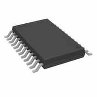
AD7192BRUZ Analog Devices Inc, AD7192BRUZ Datasheet - Page 6

AD7192BRUZ
Manufacturer Part Number
AD7192BRUZ
Description
IC ADC 24BIT 2CH W/PGA 24-TSSOP
Manufacturer
Analog Devices Inc
Datasheet
1.AD7192BRUZ.pdf
(40 pages)
Specifications of AD7192BRUZ
Data Interface
DSP, MICROWIRE™, QSPI™, Serial, SPI™
Design Resources
Precision Weigh Scale Design Using AD7192 with Internal PGA (CN0119)
Number Of Bits
24
Sampling Rate (per Second)
4.8k
Number Of Converters
1
Voltage Supply Source
Analog and Digital
Operating Temperature
-40°C ~ 105°C
Mounting Type
Surface Mount
Package / Case
24-TSSOP (0.173", 4.40mm Width)
Resolution (bits)
24bit
Input Channel Type
Pseudo Differential
Supply Voltage Range - Analogue
3V To 5.25V
Supply Voltage Range - Digital
2.7V To 5.25V
Supply
RoHS Compliant
Sampling Rate
4.8kSPS
Rohs Compliant
Yes
Lead Free Status / RoHS Status
Lead free / RoHS Compliant
Available stocks
Company
Part Number
Manufacturer
Quantity
Price
Company:
Part Number:
AD7192BRUZ
Manufacturer:
ADI
Quantity:
1 000
Company:
Part Number:
AD7192BRUZ
Manufacturer:
AD
Quantity:
1 831
Company:
Part Number:
AD7192BRUZ
Manufacturer:
ADI
Quantity:
325
Part Number:
AD7192BRUZ
Manufacturer:
ADI/亚德诺
Quantity:
20 000
Company:
Part Number:
AD7192BRUZ-REEL
Manufacturer:
ADI
Quantity:
1 000
AD7192
Parameter
SYSTEM CALIBRATION
POWER REQUIREMENTS
1
2
3
4
5
6
7
Temperature range: −40°C to +105°C.
Specification is not production tested but is supported by characterization data at initial product release.
FS is the decimal equivalent of Bit FS9 to Bit FS0 in the mode register.
Following a system or internal zero-scale calibration, the offset error is in the order of the noise for the programmed gain and output data rate selected. A system full-
scale calibration reduces the gain error to the order of the noise for the programmed gain and output data rate.
The analog inputs are configured for differential mode.
REJ60 is a bit in the mode register. When the output data rate is set to 50 Hz, setting REJ60 to 1 places a notch at 60 Hz, allowing simultaneous 50 Hz/60 Hz rejection.
Digital inputs equal to DV
Full-Scale Calibration Limit
Zero-Scale Calibration Limit
Input Span
Power Supply Voltage
AV
DV
Power Supply Currents
AI
DI
I
DD
DD
DD
DD
DD
(Power-Down Mode)
Current
Current
− AGND
− DGND
2
DD
7
or DGND.
AD7192B
1.05 × FS
−1.05 × FS
0.8 × FS
2.1 × FS
3/5.25
2.7/5.25
0.6
0.85
3.2
3.6
4.5
5
0.4
0.6
1.5
3
Rev. A | Page 6 of 40
Unit
V max
V min
V min
V max
V min/max
V min/max
mA max
mA max
mA max
mA max
mA max
mA max
mA max
mA max
mA typ
μA max
Test Conditions/Comments
0.53 mA typical, gain = 1, buffer off.
0.75 mA typical, gain = 1, buffer on.
2.5 mA typical, gain = 8, buffer off.
3 mA typical, gain = 8, buffer on.
3.5 mA typical, gain = 16 to 128, buffer off.
4 mA typical, gain = 16 to 128, buffer on.
0.35 mA typical, DV
0.5 mA typical, DV
External crystal used.
DD
DD
= 5 V.
= 3 V.
1


