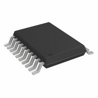
AD7866ARUZ Analog Devices Inc, AD7866ARUZ Datasheet - Page 7

AD7866ARUZ
Manufacturer Part Number
AD7866ARUZ
Description
IC ADC 12BIT 2CH DUAL 20-TSSOP
Manufacturer
Analog Devices Inc
Datasheet
1.AD7866ARU-REEL.pdf
(24 pages)
Specifications of AD7866ARUZ
Data Interface
DSP, MICROWIRE™, QSPI™, Serial, SPI™
Number Of Bits
12
Sampling Rate (per Second)
1M
Number Of Converters
2
Power Dissipation (max)
24mW
Voltage Supply Source
Analog and Digital
Operating Temperature
-40°C ~ 125°C
Mounting Type
Surface Mount
Package / Case
20-TSSOP (0.173", 4.40mm Width)
Resolution (bits)
12bit
Input Channel Type
Single Ended
Supply Voltage Range - Analogue
2.7V To 5.25V
Supply Voltage Range - Digital
2.7V To 5.25V
Supply
RoHS Compliant
Sampling Rate
1MSPS
Rohs Compliant
Yes
Number Of Elements
2
Resolution
12Bit
Architecture
SAR
Sample Rate
1MSPS
Input Polarity
Unipolar
Input Type
Voltage
Rated Input Volt
2.5/5V
Differential Input
No
Power Supply Requirement
Analog and Digital
Single Supply Voltage (typ)
3/5V
Single Supply Voltage (min)
2.7V
Single Supply Voltage (max)
5.25V
Dual Supply Voltage (typ)
Not RequiredV
Dual Supply Voltage (min)
Not RequiredV
Dual Supply Voltage (max)
Not RequiredV
Power Dissipation
24mW
Differential Linearity Error
-0.95LSB/1.25LSB
Integral Nonlinearity Error
±1.5LSB
Operating Temp Range
-40C to 125C
Operating Temperature Classification
Automotive
Mounting
Surface Mount
Pin Count
20
Package Type
TSSOP
Input Signal Type
Single-Ended
Lead Free Status / RoHS Status
Lead free / RoHS Compliant
For Use With
EVAL-AD7866CBZ - BOARD EVALUATION AD7866
Lead Free Status / Rohs Status
Compliant
Available stocks
Company
Part Number
Manufacturer
Quantity
Price
Part Number:
AD7866ARUZ
Manufacturer:
ADI/亚德诺
Quantity:
20 000
Part Number:
AD7866ARUZ-REEL7
Manufacturer:
ADI/亚德诺
Quantity:
20 000
Pin No.
11
12
13
14
15, 16
17
18
19
20
REV. A
Mnemonic
RANGE
AV
DV
DGND
D
V
SCLK
CS
A0
DRIVE
OUT
DD
DD
A, D
OUT
B
Function
Analog Input Range and Output Coding Selection. Logic input. The polarity on this pin will
determine what input range the analog input channels on the AD7866 will have, and will also select
the type of output coding the ADC will use for the conversion result. On the falling edge of CS, the
polarity of this pin is checked to determine the analog input range of the next conversion. If this pin
is tied to a logic low, the analog input range is 0 V to V
be straight binary (for the next conversion). If this pin is tied to a logic high when CS goes low, the
analog input range is 2
ever, if after the falling edge of CS the logic level of the RANGE pin has changed upon the eighth
SCLK falling edge, the output coding will change to the other option without any change in the
analog input range. (See the Analog Input and ADC Transfer Function sections.)
Analog Supply Voltage, 2.7 V to 5.25 V. This is the only supply voltage for all analog circuitry on the
AD7866. The AV
more than 0.3 V apart even on a transient basis. This supply should be decoupled to AGND.
Digital Supply Voltage, 2.7 V to 5.25 V. This is the supply voltage for all digital circuitry on the
AD7866. The DV
more than 0.3 V apart even on a transient basis. This supply should be decoupled to DGND.
Digital Ground. This is the ground reference point for all digital circuitry on the AD7866. The
DGND and AGND voltages ideally should be at the same potential and must not be more than 0.3 V
apart even on a transient basis.
Serial Data Outputs. The data output is supplied to this pin as a serial data stream. The bits are
clocked out on the falling edge of the SCLK input. The data appears on both pins simultaneously
from the simultaneous conversions of both ADCs. The data stream consists of one leading zero
followed by three STATUS bits, followed by the 12 bits of conversion data. The data is provided
MSB first. If CS is held low for another 16 SCLK cycles after the conversion data has been output
on either D
from a simultaneous conversion on both ADCs to be gathered in serial format on either D
D
Logic Power Supply Input. The voltage supplied at this pin determines at what voltage the interface
will operate. This pin should be decoupled to DGND.
Serial Clock. Logic Input. A serial clock input provides the SCLK for accessing the data from the
AD7866. This clock is also used as the clock source for the conversion process.
Chip Select. Active low logic input. This input provides the dual function of initiating conversions on
the AD7866 and frames the serial data transfer.
Multiplexer Select. Logic input. This input is used to select the pair of channels to be converted
simultaneously, i.e., Channel 1 of both ADC A and ADC B, or Channel 2 of both ADC A and ADC B.
The logic state of this pin is checked upon the falling edge of CS, and the multiplexer is set up for
the next conversion. If it is low, the following conversion will be performed on Channel 1 of each ADC;
if it is high, the following conversion will be performed on Channel 2 of each ADC.
OUT
B alone using only one serial port. See the Serial Interface section.
PIN FUNCTION DESCRIPTIONS (continued)
OUT
A or D
DD
DD
and DV
and AV
OUT
V
B, the data from the other ADC follows on the D
REF
DD
DD
and the output coding for the part will be twos complement. How-
voltages ideally should be at the same potential and must not be
voltages should ideally be at the same potential and must not be
–7–
REF
and the output coding from the part will
OUT
pin. This allows data
AD7866
OUT
A or


