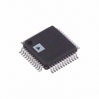
AD7651ASTZ Analog Devices Inc, AD7651ASTZ Datasheet - Page 23

AD7651ASTZ
Manufacturer Part Number
AD7651ASTZ
Description
IC ADC 16BIT 100KSPS 48-LQFP
Manufacturer
Analog Devices Inc
Series
PulSAR®r
Datasheet
1.AD7651ASTZ.pdf
(28 pages)
Specifications of AD7651ASTZ
Data Interface
Serial, Parallel
Number Of Bits
16
Sampling Rate (per Second)
100k
Number Of Converters
1
Power Dissipation (max)
45mW
Voltage Supply Source
Analog and Digital
Operating Temperature
-40°C ~ 85°C
Mounting Type
Surface Mount
Package / Case
48-LQFP
Resolution (bits)
16bit
Input Channel Type
Pseudo Differential
Supply Voltage Range - Analogue
4.75V To 5.25V
Supply Voltage Range - Digital
2.7V To 5.25V,
Sampling Rate
100kSPS
Rohs Compliant
Yes
Lead Free Status / RoHS Status
Lead free / RoHS Compliant
For Use With
EVAL-AD7651CBZ - BOARD EVALUATION FOR AD7651
Lead Free Status / RoHS Status
Lead free / RoHS Compliant, Lead free / RoHS Compliant
Available stocks
Company
Part Number
Manufacturer
Quantity
Price
Company:
Part Number:
AD7651ASTZ
Manufacturer:
Analog Devices Inc
Quantity:
10 000
External Discontinuous Clock Data Read After
Conversion
Though the maximum throughput cannot be achieved using
this mode, it is the most recommended of the serial slave modes.
Figure 34
After a conversion is complete, indicated by BUSY returning
LOW, the conversion’s result can be read while both CS and RD
are LOW. Data is shifted out MSB first with 16 clock pulses and
is valid on the rising and falling edges of the clock.
Among the advantages of this method is the fact that conversion
performance is not degraded because there are no voltage
transients on the digital interface during the conversion process.
Another advantage is the ability to read the data at any speed up
to 40 MHz, which accommodates both the slow digital host
interface and the fastest serial reading.
Finally, in this mode only, the AD7651 provides a daisy-chain
feature using the RDC/SDIN pin for cascading multiple con-
verters together. This feature is useful for reducing component
count and wiring connections when desired, as, for instance, in
isolated multiconverter applications.
An example of the concatenation of two devices is shown in
Figure 36
common CNVST signal. It should be noted that the RDC/SDIN
input is latched on the opposite edge of SCLK of the one used to
shift out the data on SDOUT. Therefore, the MSB of the
“upstream” converter just follows the LSB of the “downstream”
converter on the next SCLK cycle.
CNVST IN
SCLK IN
CS IN
RDC/SDIN
(UPSTREAM)
AD7651
Figure 36. Two AD7651s in a Daisy-Chain Configuration
. Simultaneous sampling is possible by using a
shows the detailed timing diagrams of this method.
BUSY
#2
CNVST
SDOUT
SCLK
CS
RDC/SDIN
(DOWNSTREAM)
AD7651
BUSY
#1
CNVST
SDOUT
SCLK
CS
02964-0-019
BUSY
OUT
DATA
OUT
Rev. 0 | Page 23 of 28
External Clock Data Read During Conversion
Figure 35 shows the detailed timing diagrams of this method.
During a conversion, while both CS and RD are LOW, the result
of the previous conversion can be read. The data is shifted out
MSB first with 16 clock pulses, and is valid on both the rising
and falling edges of the clock. The 16 bits must be read before
the current conversion is complete; otherwise, RDERROR is
pulsed HIGH and can be used to interrupt the host interface to
prevent incomplete data reading. There is no daisy-chain feature
in this mode and the RDC/SDIN input should always be tied
either HIGH or LOW.
To reduce performance degradation due to digital activity, a fast
discontinuous clock of at least 18 MHz is recommended to
ensure that all the bits are read during the first half of the
conversion phase. It is also possible to begin to read data after
conversion and continue to read the last bits after a new
conversion has been initiated. This allows the use of a slower
clock speed like 14 MHz.
AD7651


