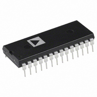
AD976ANZ Analog Devices Inc, AD976ANZ Datasheet - Page 8

AD976ANZ
Manufacturer Part Number
AD976ANZ
Description
IC ADC 16BIT 100KSPS 28-DIP
Manufacturer
Analog Devices Inc
Datasheet
1.AD976ANZ.pdf
(16 pages)
Specifications of AD976ANZ
Data Interface
Parallel
Number Of Bits
16
Sampling Rate (per Second)
200k
Number Of Converters
1
Power Dissipation (max)
100mW
Voltage Supply Source
Analog and Digital
Operating Temperature
-40°C ~ 85°C
Mounting Type
Through Hole
Package / Case
28-DIP (0.600", 15.24mm)
Resolution (bits)
16bit
Sampling Rate
100kSPS
Input Channel Type
Single Ended
Supply Voltage Range - Analog
4.75V To 5.25V
Supply Voltage Range - Digital
4.75V To 5.25V
Supply Voltage Range - Analogue
4.75V To 5.25V
Rohs Compliant
Yes
Number Of Elements
1
Resolution
16Bit
Architecture
SAR
Sample Rate
100KSPS
Input Polarity
Bipolar
Input Type
Voltage
Rated Input Volt
±10V
Differential Input
No
Power Supply Requirement
Analog and Digital
Single Supply Voltage (typ)
5V
Single Supply Voltage (min)
4.75V
Single Supply Voltage (max)
5.25V
Dual Supply Voltage (typ)
Not RequiredV
Dual Supply Voltage (min)
Not RequiredV
Dual Supply Voltage (max)
Not RequiredV
Power Dissipation
100mW
Differential Linearity Error
-2LSB/3LSB
Integral Nonlinearity Error
±3LSB
Operating Temp Range
-40C to 85C
Operating Temperature Classification
Industrial
Mounting
Through Hole
Pin Count
28
Package Type
PDIP W
Input Signal Type
Single-Ended
Lead Free Status / RoHS Status
Lead free / RoHS Compliant
For Use With
EVAL-AD976CB - BOARD EVAL FOR AD976EVAL-AD976ACB - BOARD EVAL FOR AD976A
Lead Free Status / Rohs Status
Compliant
Available stocks
Company
Part Number
Manufacturer
Quantity
Price
Company:
Part Number:
AD976ANZ
Manufacturer:
Analog Devices Inc
Quantity:
135
Company:
Part Number:
AD976ANZ
Manufacturer:
DENSO
Quantity:
6 255
Part Number:
AD976ANZ
Manufacturer:
ADI/亚德诺
Quantity:
20 000
AD976/AD976A
CONVERSION CONTROL
The AD976/AD976A is controlled by two signals: R/C and CS,
as shown in Figures 2 and 3. To initiate a conversion and place
the sample/hold circuit into the hold state, both the R/C and CS
signals must be brought low for no less than 50 ns. Once the
conversion process begins, the BUSY signal will go Low until
the conversion is complete. At the end of a conversion, BUSY
will return High, and the resulting valid data will be available on
the data bus. On the first conversion after the AD976/AD976A
is powered up, the DATA output will be indeterminate.
The AD976/AD976A exhibits two modes of conversion. In the
mode demonstrated in Figure 2, conversion timing is controlled
by a negative-going R/C signal, at least 50 ns wide. In this mode
the CS pin is always tied low, and the only limit placed on how
long the R/C signal can remain low is the desired sampling rate.
Less than 83 ns after the initiation of a conversion, the BUSY
signal will be brought low and remain low until the conversion is
complete and the output shift registers have been updated with
the new Binary Twos Complement data.
Figure 2. Conversion Timing with Outputs Enabled After Conversion ( CS Tied Low)
MODE
BUSY
DATA
BUS
R/C
CS
MODE
BUSY
DATA
BUS
R/C
ACQUIRE
Figure 3. Using CS to Control Conversion and Read Timing
t
12
DATA VALID
ACQUIRE
PREVIOUS
t
1
t
6
t
3
t
t
9
3
t
t
1
6
HI-Z
t
12
t
t
14
11
CONVERT
CONVERT
DATA VALID
t
t
PREVIOUS
7
4
t
t
2
7
t
–8–
4
t
13
Figure 3 demonstrates the AD976/AD976A conversion timing,
using CS to control both the conversion process and the reading
of output data. To operate in this mode, the R/C signal should
be brought low no less than 10 ns before the falling edge of a CS
pulse (50 ns wide) is applied to the ADC. Once these two pulses
are applied, BUSY will go low and remain low until a conver-
sion is complete. After a maximum of 4 s (AD976A only),
BUSY will again return high, and parallel data will be valid on
the ADC outputs. To achieve the maximum 100 kHz/200 kHz
throughput rate of the part, the negative going R/C and CS
control signals should be applied every 5 s (AD976A). It should
also be noted that although all R/C and CS commands will be
ignored once a conversion has begun, these inputs can be
asserted during a conversion; i.e., a read during conversion can
be performed. Voltage transients on these inputs could feed
through to the analog circuitry and affect conversion results.
VALID
NOT
t
ACQUIRE
5
HI-Z
DATA
VALID
ACQUIRE
t
8
t
t
10
12
t
14
HI-Z
t
1
DATA VALID
CONVERT
t
VALID
DATA
t
9
12
HI-Z
REV. C


