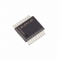
MAX147BCAP+ Maxim Integrated Products, MAX147BCAP+ Datasheet - Page 20

MAX147BCAP+
Manufacturer Part Number
MAX147BCAP+
Description
IC SRL ADC 8CH 12BIT 2.7V 20SSOP
Manufacturer
Maxim Integrated Products
Datasheet
1.MAX147BCAP.pdf
(24 pages)
Specifications of MAX147BCAP+
Number Of Bits
12
Sampling Rate (per Second)
133k
Data Interface
MICROWIRE™, QSPI™, Serial, SPI™
Number Of Converters
1
Power Dissipation (max)
640mW
Voltage Supply Source
Single Supply
Operating Temperature
0°C ~ 70°C
Mounting Type
Surface Mount
Package / Case
20-SSOP
Architecture
SAR
Conversion Rate
133 KSPs
Resolution
12 bit
Interface Type
4-Wire (SPI, QSPI, MICROWIRE, TMS320)
Voltage Reference
Internal 2.5 V or External
Supply Voltage (max)
5.25 V
Supply Voltage (min)
2.7 V
Mounting Style
SMD/SMT
Lead Free Status / RoHS Status
Lead free / RoHS Compliant
+2.7V, Low-Power, 8-Channel,
Serial 12-Bit ADCs
VREF, the DC input resistance is a minimum of 18kΩ.
During conversion, an external reference at VREF must
deliver up to 350µA DC load current and have 10Ω or
less output impedance. If the reference has a higher
output impedance or is noisy, bypass it close to the
VREF pin with a 4.7µF capacitor.
Using the REFADJ input makes buffering the external
reference unnecessary. To use the direct VREF input,
disable the internal buffer by tying REFADJ to V
power-down, the input bias current to REFADJ is typi-
cally 25µA (MAX146) with REFADJ tied to V
REFADJ to AGND to minimize the input bias current in
power-down.
Table 7 shows the full-scale voltage ranges for unipolar
and bipolar modes.
The external reference must have a temperature coeffi-
cient of 4ppm/°C or less to achieve accuracy to within
1LSB over the 0°C to +70°C commercial temperature
range.
Figure 17 depicts the nominal, unipolar input/output
(I/O) transfer function, and Figure 18 shows the bipolar
input/output transfer function. Code transitions occur
halfway between successive-integer LSB values.
Output coding is binary, with 1LSB = 610µV (2.500V /
4096) for unipolar operation, and 1LSB = 610µV
[(2.500V / 2 - -2.500V / 2) / 4096] for bipolar operation.
For best performance, use printed circuit boards.
Wire-wrap boards are not recommended. Board layout
should ensure that digital and analog signal lines are
separated from each other. Do not run analog and digi-
tal (especially clock) lines parallel to one another, or
digital lines underneath the ADC package.
Figure 19 shows the recommended system ground
connections. Establish a single-point analog ground
(star ground point) at AGND, separate from the logic
ground. Connect all other analog grounds and DGND
to the star ground. No other digital system ground
should be connected to this ground. For lowest-noise
operation, the ground return to the star ground’s power
Table 7. Full Scale and Zero Scale
20
______________________________________________________________________________________
VREF + COM
Full Scale
Layout, Grounding, and Bypassing
UNIPOLAR MODE
Transfer Function
Zero Scale
COM
DD
DD
. Pull
. In
supply should be low impedance and as short as
possible.
High-frequency noise in the V
affect the high-speed comparator in the ADC. Bypass
the supply to the star ground with 0.1µF and 1µF
capacitors close to pin 20 of the MAX146/MAX147.
Minimize capacitor lead lengths for best supply-noise
rejection. If the power supply is very noisy, a 10Ω resis-
tor can be connected as a lowpass filter (Figure 19).
The MAX146/MAX147 can interface with QSPI using
the circuit in Figure 20 (f
CPHA = 0). This QSPI circuit can be programmed to do a
conversion on each of the eight channels. The result is
stored in memory without taxing the CPU, since QSPI
incorporates its own microsequencer.
The MAX146/MAX147 are QSPI compatible up to the
maximum external clock frequency of 2MHz.
Figure 17. Unipolar Transfer Function, Full Scale (FS) = VREF
+ COM, Zero Scale (ZS) = COM
Full Scale
11 . . . 111
11 . . . 110
High-Speed Digital Interfacing with QSPI
11 . . . 101
00 . . . 011
00 . . . 010
00 . . . 001
VREF / 2
00 . . . 000
Positive
+ COM
OUTPUT CODE
(COM)
0
1
2
INPUT VOLTAGE (LSB)
BIPOLAR MODE
3
Scale
COM
Zero
SCLK
FULL-SCALE
TRANSITION
DD
= 2.0MHz, CPOL = 0,
power supply may
FS - 3/2LSB
Full Scale
-VREF / 2
Negative
+ COM
ZS = COM
1LSB =
FS = VREF + COM
FS
VREF
4096


