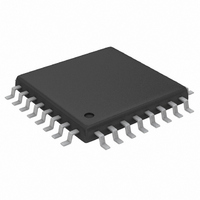
MAX1498ECJ+ Maxim Integrated Products, MAX1498ECJ+ Datasheet - Page 18

MAX1498ECJ+
Manufacturer Part Number
MAX1498ECJ+
Description
IC ADC 4 1/2DIG W/LED DVR 32TQFP
Manufacturer
Maxim Integrated Products
Datasheet
1.MAX1496EAI.pdf
(24 pages)
Specifications of MAX1498ECJ+
Number Of Bits
4.5 Digit
Sampling Rate (per Second)
5
Number Of Converters
1
Power Dissipation (max)
1.65W
Voltage Supply Source
Analog and Digital
Operating Temperature
-40°C ~ 85°C
Mounting Type
Surface Mount
Package / Case
32-LQFP
Lead Free Status / RoHS Status
Lead free / RoHS Compliant
A resistor from ISET to ground sets the current for each
LED segment. See Table 5 for more detail. Use the fol-
lowing formula to set the segment current:
R
the internal current-limit circuit limits the I
30mA. At higher I
device is not guaranteed. In addition, the power dissipat-
ed may exceed the package power-dissipation limit.
The MAX1447/MAX1496/MAX1498 drive a peak current
of 25.5mA into LEDs with a 2.2V forward voltage drop
when operated from a supply voltage of at least 3.0V.
Therefore, the minimum voltage drop across the inter-
nal LED drivers is (3.0V - 2.2V) = 0.8V. The MAX1447/
MAX1496/MAX1498 sink (8 x 25.5mA = 204mA) when
the outputs are operating and the LED segment drivers
are at full current. For a 3.3V supply, the MAX1447/
MAX1496/MAX1498 dissipate (3.3V - 2.2V) x 204 =
224.4mW. If a higher supply voltage is used, the driver
absorbs a higher voltage, and the driver’s power dissi-
pation increases accordingly. However, if the LEDs
used have a higher forward voltage drop than 2.2V, the
supply voltage must be raised accordingly to ensure
that the driver always has at least 0.8V headroom.
For a VLED supply voltage of 2.7V, the maximum LED
forward voltage is 1.9V to ensure 0.8V driver headroom.
The voltage drop across the drivers with a nominal +5V
supply (5.0V - 2.2V = 2.8V) is almost three times the
drop across the drivers with a nominal 3.3V supply
(3.3V - 2.2V = 1.1V). Therefore, the driver’s power dissi-
pation increases three times. The power dissipation in
the part causes the junction temperature to rise accord-
ingly. In the high ambient temperature case, the total
junction temperature may be very high (>+125°C). At
higher junction temperatures, the ADC performance
degrades. To ensure the dissipation limit for the
MAX1447/MAX1496/MAX1498 is not exceeded and the
ADC performance is not degraded, a diode can be
inserted between the power supply and VLED.
3.5- and 4.5-Digit, Single-Chip ADCs
with LED Drivers
18
ISET
______________________________________________________________________________________
values below 25kΩ increase the I
Choosing Supply Voltage to Minimize
I
SEG
SEG
Selecting Segment Current
=
values, proper operation of the
1 20
R
.
ISET
V
×
Power Dissipation
450
SEG
SEG
to less than
. However,
Computing Power Dissipation
The following can be used to compute power dissipation:
VLED = LED driver supply voltage
I
V
DUTY = segment ON time during each digit ON time
I
N = number of segments driven (worst case is eight)
V
I
AV
For I
1.5V at 25.5mA, VLED = V
For the 28-pin SSOP package (T
+105.3°C/W), the maximum allowed ambient tempera-
ture T
Thus, the device cannot operate safely at a maximum
package temperature of +85°C. The power dissipates
in the part need to be lowered.
Table 5. Segment-Current Selection
VLED
SEG
SUPPLY
DIODE
SUPPLY
DD
SEG
= segment current set by R
PD = (5.25 x 2mA) + (5.25V - 1.5) [(127 / 128)
A
= VLED bias current
+ DV
R
+125°C = T
PD = (VLED x I
is given by:
ISET
= LED forward voltage
>2500
= supply current from V
= 25.5mA, N = 8, DUTY = 127 / 128, V
= supply voltage of the part
100
500
25
50
DD
x 25.5mA x 8)] + 5.25 x 1.080mA
(kΩ)
(DUTY x I
T
J
for the MAX1447/MAX1498.
(max) = T
A
PD = 0.7751W
+ (0.7751W x +105.3°C/W)
T
28-Pin SSOP-Package Example
VLED
SEG
A
= +43°C
A
SUPPLY
x N) + V
+ (PD x T
) + (VLED - V
LED driver disabled
ISET
DD
Dissipation Example
= 5.25V:
JA
I
SEG
SUPPLY
for the MAX1496 or
JA
21.6
10.8
= 1 / 0.009496 =
5.4
1.1
(mA)
) =
DIODE
x I
SUPPLY
DIODE
)
=


