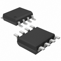
MAX1241AESA+ Maxim Integrated Products, MAX1241AESA+ Datasheet - Page 10

MAX1241AESA+
Manufacturer Part Number
MAX1241AESA+
Description
IC ADC SRL 12BIT 2.7V 8-SOIC
Manufacturer
Maxim Integrated Products
Datasheet
1.MAX1241BCSA.pdf
(15 pages)
Specifications of MAX1241AESA+
Number Of Bits
12
Sampling Rate (per Second)
73k
Data Interface
MICROWIRE™, QSPI™, Serial, SPI™
Number Of Converters
1
Power Dissipation (max)
471mW
Voltage Supply Source
Single Supply
Operating Temperature
-40°C ~ 85°C
Mounting Type
Surface Mount
Package / Case
8-SOIC (0.154", 3.90mm Width)
Lead Free Status / RoHS Status
Lead free / RoHS Compliant
+2.7V, Low-Power,
12-Bit Serial ADCs in 8-Pin SO
Power consumption can be reduced significantly by
shutting down the MAX1240/MAX1241 between con-
versions. Figure 6 shows a plot of average supply cur-
rent versus conversion rate. Because the MAX1241
uses an external reference voltage (assumed to be pre-
sent continuously), it “wakes up” from shutdown more
quickly (in 4µs) and therefore provides lower average
supply currents. The wake-up time (t
from when SHDN is deasserted to the time when a con-
version may be initiated (Figure 5). For the MAX1240,
this time depends on the time in shutdown (Figure 7)
because the external 4.7µF reference bypass capacitor
loses charge slowly during shutdown.
The actual conversion does not require the external
clock. This allows the conversion result to be read back
at the µP’s convenience at any clock rate from up to
2.1MHz. The clock duty cycle is unrestricted if each
clock phase is at least 200ns. Do not run the clock
while a conversion is in progress.
Conversion-start and data-read operations are controlled
by the CS and SCLK digital inputs. The timing diagrams
of Figures 8 and 9 outline serial-interface operation.
A CS falling edge initiates a conversion sequence: the
T/H stage holds the input voltage, the ADC begins to
convert, and DOUT changes from high impedance to
logic low. SCLK must be kept low during the conver-
sion. An internal register stores the data when the con-
version is in progress.
10
Figure 8. Interface Timing Sequence
______________________________________________________________________________________
TRACK/HOLD
STATE
DOUT
INTERFACE IDLE
CYCLE TIME
SCLK
Using SHDN to Reduce Supply Current
CS
TRACK
IN PROGRESS
CONVERSION
7.5μs (t
HOLD
CONV
)
Timing and Control
EOC
0μs
External Clock
EOC
WAKE
1
) is the time
B11 B10 B9
4
B8
CLOCK OUT SERIAL DATA
12.5 × 0.476μs = 5.95μs
TOTAL = 13.7μs
B7
B6
Figure 6. Average Supply Current vs. Conversion Rate
Figure 7. Typical Reference Power-Up Delay vs. Time in
Shutdown
B5
8
TRACK
B4
B3
0.001
0.01
0.8
0.6
0.4
0.2
0.0
1.0
0.1
10
B2
0.001
1
0.1
B1
V
R
CODE = 010101010000
12
DD =
LOAD
1
B0
V
= ∞, C
0.01
REF
TIME IN SHUTDOWN (sec)
CONVERSION RATE (Hz)
= 3.0V
10
MAX1240
LOAD
TRAILING
ZEROS
0μs
= 50pF
100
0.1
16
MAX1241
1k
1
0.24μs
(t
10k
CS
IDLE
)
100k
10
HOLD


