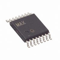
MAX1082AEUE+ Maxim Integrated Products, MAX1082AEUE+ Datasheet - Page 13

MAX1082AEUE+
Manufacturer Part Number
MAX1082AEUE+
Description
IC ADC 10BIT 400KSPS 16-TSSOP
Manufacturer
Maxim Integrated Products
Datasheet
1.MAX1082BEUE.pdf
(24 pages)
Specifications of MAX1082AEUE+
Number Of Bits
10
Sampling Rate (per Second)
400k
Data Interface
MICROWIRE™, QSPI™, Serial, SPI™
Number Of Converters
1
Power Dissipation (max)
533mW
Voltage Supply Source
Single Supply
Operating Temperature
-40°C ~ 85°C
Mounting Type
Surface Mount
Package / Case
16-TSSOP
Lead Free Status / RoHS Status
Lead free / RoHS Compliant
Table 1. Channel Selection in Single-Ended Mode (SGL /
Table 2. Channel Selection in Pseudo-Differential Mode (SGL / DIF = 0)
The external clock not only shifts data in and out, but it
also drives the analog-to-digital conversion steps.
SSTRB pulses high for one clock period after the last bit
of the control byte. Successive-approximation bit deci-
sions are made and appear at DOUT on each of the
next 12 SCLK falling edges, MSB first (Figure 5). SSTRB
and DOUT go into a high-impedance state when CS
goes high; after the next CS falling edge, SSTRB out-
puts a logic low. Figure 6 shows the detailed serial-inter-
face timings.
The conversion must complete in 120µs or less, or
droop on the sample-and-hold capacitors may degrade
conversion results.
The falling edge of CS does not start a conversion.
The first logic high clocked into DIN is interpreted as a
start bit and defines the first bit of the control byte. A
conversion starts on SCLK’s falling edge, after the eighth
bit of the control byte (the PD0 bit) is clocked into DIN.
The start bit is defined as follows:
Once a start bit has been recognized, the current conver-
sion may only be terminated by pulling SHDN low.
SEL2
The first high bit clocked into DIN with CS low any
time the converter is idle; e.g., after V
are applied.
The first high bit clocked into DIN after bit B4 of a
conversion in progress is clocked onto the DOUT pin
(Figure 7).
SEL2
0
1
0
1
0
0
1
1
SEL1
______________________________________________________________________________________
0
0
1
1
SEL1
0
1
0
1
OR
SEL0
1
1
0
0
Data Framing
SEL0
Serial Clock
DD1
1
0
1
0
and V
CH0
+
DD2
CH0
+
–
The fastest the MAX1082/MAX1083 can run with CS held
low between conversions is 16 clocks per conversion.
Figure 7 shows the serial-interface timing necessary to
perform a conversion every 16 SCLK cycles. If CS is tied
low and SCLK is continuous, guarantee a start bit by first
clocking in 16 zeros.
__________ Applications Information
When power is first applied, and if SHDN is not pulled
low, internal power-on reset circuitry activates the
MAX1082/MAX1083 in normal operating mode, ready to
convert with SSTRB = low. After the power supplies sta-
bilize, the internal reset time is 10µs, and no conver-
sions should be performed during this phase. If CS is
low, the first logic 1 on DIN is interpreted as a start bit.
Until a conversion takes place, DOUT shifts out zeros.
Additionally, wait for the reference to stabilize when
using the internal reference.
Save power by placing the converter in one of two low-
current operating modes or in full power-down between
conversions. Select the power mode through bit 1 and
bit 0 of the DIN control byte (Tables 3 and 4), or force
the converter into hardware shutdown by driving SHDN
to GND.
The software power-down modes take effect after the
conversion is completed; SHDN overrides any software
power mode and immediately stops any conversion in
progress. In software power-down mode, the serial
interface remains active while waiting for a new control
byte to start conversion and switch to full-power mode.
CH1
+
DIF = 1)
CH1
+
–
CH2
+
CH2
+
–
CH3
+
Power-On Reset
Power Modes
CH3
COM
+
–
–
–
–
–
13


