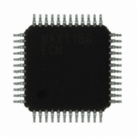
MAX1185ECM+D Maxim Integrated Products, MAX1185ECM+D Datasheet

MAX1185ECM+D
Specifications of MAX1185ECM+D
Related parts for MAX1185ECM+D
MAX1185ECM+D Summary of contents
Page 1
... High Resolution Imaging I/Q Channel Digitization Multichannel IF Sampling Instrumentation Video Application Ultrasound ________________________________________________________________ Maxim Integrated Products For pricing, delivery, and ordering information, please contact Maxim Direct at 1-888-629-4642, or visit Maxim’s website at www.maxim-ic.com. o Single 3V Operation o Excellent Dynamic Performance: 59.5dB SNR at f 74dB SFDR at f ...
Page 2
Dual 10-Bit, 20Msps, 3V, Low-Power ADC with Internal Reference and Multiplexed Parallel Outputs ABSOLUTE MAXIMUM RATINGS GND ...............................................-0.3V to +3. OGND to GND.......................................................-0.3V to +0.3V INA+, INA-, INB+, INB- to GND ...............................-0. ...
Page 3
Dual 10-Bit, 20Msps, 3V, Low-Power ADC with Internal Reference and Multiplexed Parallel Outputs ELECTRICAL CHARACTERISTICS (continued 3V 2.5V, 0.1µF and 1µF capacitors from REFP, REFN, and COM to GND; REFOUT connected to REFIN through a DD ...
Page 4
Dual 10-Bit, 20Msps, 3V, Low-Power ADC with Internal Reference and Multiplexed Parallel Outputs ELECTRICAL CHARACTERISTICS (continued 3V 2.5V, 0.1µF and 1µF capacitors from REFP, REFN, and COM to GND; REFOUT connected to REFIN through a DD ...
Page 5
Dual 10-Bit, 20Msps, 3V, Low-Power ADC with Internal Reference and Multiplexed Parallel Outputs ELECTRICAL CHARACTERISTICS (continued 3V 2.5V, 0.1µF and 1µF capacitors from REFP, REFN, and COM to GND; REFOUT connected to REFIN through a DD ...
Page 6
Dual 10-Bit, 20Msps, 3V, Low-Power ADC with Internal Reference and Multiplexed Parallel Outputs ( 2.5V 2.048V, differential input at -0.5dBFS REFIN FFT PLOT CHA (DIFFERENTIAL INPUT, 8192-POINT DATA RECORD ...
Page 7
Dual 10-Bit, 20Msps, 3V, Low-Power ADC with Internal Reference and Multiplexed Parallel Outputs ( 2.5V 2.048V, differential input at -0.5dBFS REFIN FULL-POWER INPUT BANDWIDTH vs. ANALOG INPUT FREQUENCY, SINGLE-ENDED 6 4 ...
Page 8
Dual 10-Bit, 20Msps, 3V, Low-Power ADC with Internal Reference and Multiplexed Parallel Outputs ( 2.5V 2.048V, differential input at -0.5dBFS REFIN OFFSET ERROR vs. TEMPERATURE 0.2 0.1 0 -0.1 CHB -0.2 ...
Page 9
Dual 10-Bit, 20Msps, 3V, Low-Power ADC with Internal Reference and Multiplexed Parallel Outputs PIN NAME Common-Mode Voltage Input/Output. Bypass to GND with a ≥ 0.1µF capacitor. 1 COM Analog Supply Voltage. Bypass each supply pin to GND with a 0.1µF ...
Page 10
Dual 10-Bit, 20Msps, 3V, Low-Power ADC with Internal Reference and Multiplexed Parallel Outputs PIN NAME Three-State Digital Output, Bit 6. Depending on status of A/B, output data reflects channel A 41 D6A/B or channel B data. Three-State Digital Output, Bit ...
Page 11
Dual 10-Bit, 20Msps, 3V, Low-Power ADC with Internal Reference and Multiplexed Parallel Outputs V IN Σ T/H FLASH DAC ADC 1.5 BITS STAGE 1 STAGE 2 DIGITAL CORRECTION LOGIC T/H V INA Figure 1. Pipelined Architecture—Stage Blocks S4a INA+ INA- ...
Page 12
Dual 10-Bit, 20Msps, 3V, Low-Power ADC with Internal Reference and Multiplexed Parallel Outputs Analog Inputs and Reference The full-scale range of the MAX1185 is determined by the internally generated voltage difference between REFP ( ...
Page 13
Dual 10-Bit, 20Msps, 3V, Low-Power ADC with Internal Reference and Multiplexed Parallel Outputs CHA CHB t CLK CLK t t DOB DOA A/B CHB CHA CHB t DA/B D0A/B-D9A/B D0B D1A D1B Figure 3. Timing Diagram ...
Page 14
Dual 10-Bit, 20Msps, 3V, Low-Power ADC with Internal Reference and Multiplexed Parallel Outputs Table 1. MAX1185 Output Codes For Differential Inputs DIFFERENTIAL INPUT VOLTAGE 511/512 +FULL SCALE - 1LSB REF V x 1/512 REF ...
Page 15
Dual 10-Bit, 20Msps, 3V, Low-Power ADC with Internal Reference and Multiplexed Parallel Outputs 300Ω 300Ω 300Ω +5V 0.1µF INPUT MAX4108 0.1µF -5V 300Ω 300Ω 300Ω 300Ω +5V 0.1µF INPUT MAX4108 0.1µF -5V 300Ω 300Ω Figure 5. Typical Application for Single-Ended-to-Differential ...
Page 16
Dual 10-Bit, 20Msps, 3V, Low-Power ADC with Internal Reference and Multiplexed Parallel Outputs 0.1µ N.C. 0.1µ N.C. Figure 6. Transformer-Coupled Input Drive Static Parameter Definitions Integral Nonlinearity (INL) Integral nonlinearity is the deviation of the values ...
Page 17
Dual 10-Bit, 20Msps, 3V, Low-Power ADC with Internal Reference and Multiplexed Parallel Outputs V IN MAX4108 V IN MAX4108 Figure 7. Using an Op Amp for Single-Ended, AC-Coupled Input Drive quantization error (residual error). The ideal, theoretical minimum analog-to-digital noise ...
Page 18
Dual 10-Bit, 20Msps, 3V, Low-Power ADC with Internal Reference and Multiplexed Parallel Outputs Figure 8. Typical QAM Application, Using the MAX1185 CLK ANALOG INPUT SAMPLED DATA (T/H) HOLD TRACK T/H Figure 9. T/H Aperture Timing 18 ...
Page 19
Dual 10-Bit, 20Msps, 3V, Low-Power ADC with Internal Reference and Multiplexed Parallel Outputs V DD GND INA+ T/H INA- CLK INB+ T/H INB- REFOUT PART MAX1190 MAX1180 MAX1181 MAX1182 MAX1183 MAX1186 MAX1184 MAX1185 MAX1198 MAX1197 MAX1196 MAX1195 ______________________________________________________________________________________ PIPELINE DEC ...
Page 20
Dual 10-Bit, 20Msps, 3V, Low-Power ADC with Internal Reference and Multiplexed Parallel Outputs For the latest package outline information and land patterns www.maxim-ic.com/packages. Note that a “+”, “#”, or “-” in the package code indicates RoHS status only. ...
Page 21
... Maxim cannot assume responsibility for use of any circuitry other than circuitry entirely embodied in a Maxim product. No circuit patent licenses are implied. Maxim reserves the right to change the circuitry and specifications without notice at any time. Maxim Integrated Products, 120 San Gabriel Drive, Sunnyvale, CA 94086 408-737-7600 ____________________ 21 © 2010 Maxim Integrated Products ...


