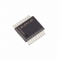
MAX146BEAP+ Maxim Integrated Products, MAX146BEAP+ Datasheet - Page 16

MAX146BEAP+
Manufacturer Part Number
MAX146BEAP+
Description
IC ADC LP 12-BIT 133KSPS 20-SSOP
Manufacturer
Maxim Integrated Products
Datasheet
1.MAX147BCAP.pdf
(24 pages)
Specifications of MAX146BEAP+
Number Of Bits
12
Sampling Rate (per Second)
133k
Data Interface
MICROWIRE™, QSPI™, Serial, SPI™
Number Of Converters
1
Power Dissipation (max)
640mW
Voltage Supply Source
Single Supply
Operating Temperature
-40°C ~ 85°C
Mounting Type
Surface Mount
Package / Case
20-SSOP
Number Of Adc Inputs
8
Architecture
SAR
Conversion Rate
133 KSPs
Resolution
12 bit
Interface Type
Serial
Voltage Reference
Internal 2.5 V or External
Supply Voltage (max)
3.3 V
Mounting Style
SMD/SMT
Lead Free Status / RoHS Status
Lead free / RoHS Compliant
+2.7V, Low-Power, 8-Channel,
Serial 12-Bit ADCs
In addition to its shutdown function, SHDN selects inter-
nal or external compensation. The compensation
affects both power-up time and maximum conversion
speed. The100kHz minimum clock rate is limited by
droop on the sample-and-hold and is independent of
the compensation used.
Float SHDN to select external compensation. The
Typical Operating Circuit uses a 4.7µF capacitor at
VREF. A 4.7µF value ensures reference-buffer stability
and allows converter operation at the 2MHz full clock
speed. External compensation increases power-up
time (see the Choosing Power-Down Mode section and
Table 4).
Pull SHDN high to select internal compensation.
Internal compensation requires no external capacitor at
VREF and allows for the shortest power-up times. The
maximum clock rate is 2MHz in internal clock mode
and 400kHz in external clock mode.
You can save power by placing the converter in a low-
current shutdown state between conversions. Select full
power-down mode or fast power-down mode via bits 1
and 0 of the DIN control byte with SHDN high or floating
(Tables 1 and 5). In both software power-down modes,
the serial interface remains operational, but the ADC
does not convert. Pull SHDN low at any time to shut
down the converter completely. SHDN overrides bits 1
and 0 of the control byte.
Full power-down mode turns off all chip functions that
draw quiescent current, reducing supply current to 2µA
(typ). Fast power-down mode turns off all circuitry
Table 4. Typical Power-Up Delay Times
16
REFERENCE
______________________________________________________________________________________
BUFFER
Disabled
Disabled
Enabled
Enabled
Enabled
Enabled
Reference-Buffer Compensation
Choosing Power-Down Mode
COMPENSATION
REFERENCE-
BUFFER
External
External
Internal
Internal
MODE
—
—
CAPACITOR
VREF
(µF)
4.7
4.7
—
—
—
—
except the bandgap reference. With fast power-down
mode, the supply current is 30µA. Power-up time can be
shortened to 5µs in internal compensation mode.
Table 4 shows how the choice of reference-buffer com-
pensation and power-down mode affects both power-up
delay and maximum sample rate. In external compensa-
tion mode, power-up time is 20ms with a 4.7µF compen-
sation capacitor when the capacitor is initially fully
discharged. From fast power-down, start-up time can be
eliminated by using low-leakage capacitors that do not
discharge more than 1/2LSB while shut down. In power-
down, leakage currents at VREF cause droop on the ref-
erence bypass capacitor. Figures 12a and 12b show
the various power-down sequences in both external and
internal clock modes.
Software power-down is activated using bits PD1 and PD0
of the control byte. As shown in Table 5, PD1 and PD0
also specify the clock mode. When software shutdown is
asserted, the ADC operates in the last specified clock
mode until the conversion is complete. Then the ADC
powers down into a low quiescent-current state. In internal
clock mode, the interface remains active and conversion
results may be clocked out after the MAX146/MAX147
enter a software power-down.
The first logical 1 on DIN is interpreted as a start bit
and powers up the MAX146/MAX147. Following
the start bit, the data input word or control byte also
determines clock mode and power-down states. For
example, if the DIN word contains PD1 = 1, then the
chip remains powered up. If PD0 = PD1 = 0, a
power-down resumes after one conversion.
POWER-DOWN
MODE
Fast
Fast
Fast
Full
Full
Full
See Figure 14c
See Figure 14c
POWER-UP
DELAY
(µs)
300
5
2
2
Software Power-Down
SAMPLING RATE
MAXIMUM
(ksps)
133
133
133
133
26
26


