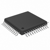
MAX1182ECM+D Maxim Integrated Products, MAX1182ECM+D Datasheet

MAX1182ECM+D
Specifications of MAX1182ECM+D
Related parts for MAX1182ECM+D
MAX1182ECM+D Summary of contents
Page 1
... High Resolution Imaging I/Q Channel Digitization Multchannel IF Undersampling Instrumentation Video Application ________________________________________________________________ Maxim Integrated Products For pricing, delivery, and ordering information, please contact Maxim Direct at 1-888-629-4642, or visit Maxim's website at www.maxim-ic.com. ♦ Single 3V Operation ♦ Excellent Dynamic Performance: 59dB SNR at f 77dB SFDR at f ♦ ...
Page 2
Dual 10-Bit, 65Msps, 3V, Low-Power ADC with Internal Reference and Parallel Outputs ABSOLUTE MAXIMUM RATINGS V , OVDD to GND...............................................-0.3V to +3.6V DD OGND to GND.......................................................-0.3V to +0.3V INA+, INA-, INB+, INB- to GND ...............................-0. REFIN, REFOUT, REFP, ...
Page 3
Dual 10-Bit, 65Msps, 3V, Low-Power ADC with Internal Reference and Parallel Outputs ELECTRICAL CHARACTERISTICS (continued 3V 2.5V; 0.1µF and 1.0µF capacitors from REFP, REFN, and COM to GND; REFOUT connected to REFIN through ...
Page 4
Dual 10-Bit, 65Msps, 3V, Low-Power ADC with Internal Reference and Parallel Outputs ELECTRICAL CHARACTERISTICS (continued 3V 2.5V; 0.1µF and 1.0µF capacitors from REFP, REFN, and COM to GND; REFOUT connected to REFIN through ...
Page 5
Dual 10-Bit, 65Msps, 3V, Low-Power ADC with Internal Reference and Parallel Outputs ELECTRICAL CHARACTERISTICS (continued 3V 2.5V; 0.1µF and 1.0µF capacitors from REFP, REFN, and COM to GND; REFOUT connected to REFIN through ...
Page 6
Dual 10-Bit, 65Msps, 3V, Low-Power ADC with Internal Reference and Parallel Outputs ( 2.5V, internal reference, differential input at -0.5dBFS noted.) FFT PLOT CHA (8192-POINT RECORD, DIFFERENTIAL INPUT 6.0065MHz CHA ...
Page 7
Dual 10-Bit, 65Msps, 3V, Low-Power ADC with Internal Reference and Parallel Outputs ( 2.5V, internal reference, differential input at -0.5dBFS noted.) TOTAL HARMONIC DISTORTION vs. ANALOG INPUT FREQUENCY -60 -64 -68 CHB -72 ...
Page 8
Dual 10-Bit, 65Msps, 3V, Low-Power ADC with Internal Reference and Parallel Outputs ( 2.5V, internal reference, differential input at -0.5dBFS noted.) DIFFERENTIAL NONLINEARITY 0.5 0.4 0.3 0.2 0.1 0 -0.1 -0.2 -0.3 -0.4 ...
Page 9
Dual 10-Bit, 65Msps, 3V, Low-Power ADC with Internal Reference and Parallel Outputs ( 2.5V, internal reference, differential input at -0.5dBFS noted.) INTERNAL REFERENCE VOLTAGE vs. TEMPERATURE 2.06 2.05 2.04 2.03 2.02 2.01 2.00 ...
Page 10
Dual 10-Bit, 65Msps, 3V, Low-Power ADC with Internal Reference and Parallel Outputs PIN NAME 21 D9B Three-State Digital Output, Bit 9 (MSB), Channel B 22 D8B Three-State Digital Output, Bit 8, Channel B 23 D7B Three-State Digital Output, Bit 7, ...
Page 11
Dual 10-Bit, 65Msps, 3V, Low-Power ADC with Internal Reference and Parallel Outputs Detailed Description The MAX1182 uses a 9-stage, fully-differential pipelined architecture (Figure 1) that allows for high- speed conversion while minimizing power consump- tion. Samples taken at the inputs ...
Page 12
Dual 10-Bit, 65Msps, 3V, Low-Power ADC with Internal Reference and Parallel Outputs S4a INA+ S4c INA- S4b S4a INB+ S4c INB- S4b Figure 2. MAX1182 T/H Amplifiers 12 ______________________________________________________________________________________ INTERNAL COM BIAS S5a S2a C1a S3a OUT C2a S1 OUT ...
Page 13
Dual 10-Bit, 65Msps, 3V, Low-Power ADC with Internal Reference and Parallel Outputs Analog Inputs and Reference The full-scale range of the MAX1182 is determined by the internally generated voltage difference between REFP ( and ...
Page 14
Dual 10-Bit, 65Msps, 3V, Low-Power ADC with Internal Reference and Parallel Outputs ANALOG INPUT CLOCK INPUT t D0 DATA OUTPUT D9A–D0A DATA OUTPUT D9B–D0B Figure 3. System Timing Diagram DISABLE ENABLE ...
Page 15
Dual 10-Bit, 65Msps, 3V, Low-Power ADC with Internal Reference and Parallel Outputs Table 1. MAX1182 Output Codes For Differential Inputs DIFFERENTIAL INPUT VOLTAGE 511/512 REF V x 1/512 REF 1/512 REF -V x 511/512 REF ...
Page 16
Dual 10-Bit, 65Msps, 3V, Low-Power ADC with Internal Reference and Parallel Outputs +5V 0.1μF INPUT MAX4108 0.1μF -5V 300Ω 300Ω +5V 0.1μF INPUT MAX4108 0.1μF -5V 300Ω 300Ω Figure 5. Typical Application for Single-Ended-to-Differential Conversion 16 ______________________________________________________________________________________ +5V 0.1μF MAX4108 ...
Page 17
Dual 10-Bit, 65Msps, 3V, Low-Power ADC with Internal Reference and Parallel Outputs Figure 6. Transformer-Coupled Input Drive Static Parameter Definitions Integral Nonlinearity (INL) Integral nonlinearity is the deviation of the values on an actual transfer function ...
Page 18
Dual 10-Bit, 65Msps, 3V, Low-Power ADC with Internal Reference and Parallel Outputs V IN MAX4108 V IN MAX4108 Figure 7. Using an Op Amp for Single-Ended, AC-Coupled Input Drive Signal-to-Noise Ratio (SNR) For a waveform perfectly reconstructed from digital samples, ...
Page 19
Dual 10-Bit, 65Msps, 3V, Low-Power ADC with Internal Reference and Parallel Outputs Figure 8. Typical QAM Application, Using the MAX1182 CLK ANALOG INPUT SAMPLED DATA (T/H) HOLD TRACK T/H Figure 9. T/H Aperture Timing ______________________________________________________________________________________ MAX2451 ...
Page 20
Dual 10-Bit, 65Msps, 3V, Low-Power ADC with Internal Reference and Parallel Outputs V DD GND INA+ T/H INA- CLK INB+ T/H INB- REFOUT PART MAX1190 MAX1180 MAX1181 MAX1182 MAX1183 MAX1186 MAX1184 MAX1185 MAX1198 MAX1197 MAX1196 MAX1195 20 ______________________________________________________________________________________ PIPELINE DEC ...
Page 21
... Maxim cannot assume responsibility for use of any circuitry other than circuitry entirely embodied in a Maxim product. No circuit patent licenses are implied. Maxim reserves the right to change the circuitry and specifications without notice at any time. Maxim Integrated Products, 120 San Gabriel Drive, Sunnyvale, CA 94086 408-737-7600 ____________________ 21 © 2006 Maxim Integrated Products Printed USA is a registered trademark of Maxim Integrated Products, Inc ...


