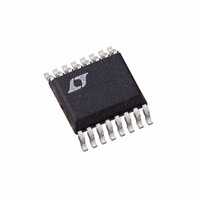
LTC1867LCGN#PBF Linear Technology, LTC1867LCGN#PBF Datasheet - Page 10

LTC1867LCGN#PBF
Manufacturer Part Number
LTC1867LCGN#PBF
Description
IC ADC 16BIT 8CH 175KSPS 16SSOP
Manufacturer
Linear Technology
Datasheet
1.LTC1863LCGNPBF.pdf
(16 pages)
Specifications of LTC1867LCGN#PBF
Number Of Bits
16
Sampling Rate (per Second)
175k
Data Interface
MICROWIRE™, Serial, SPI™
Number Of Converters
1
Power Dissipation (max)
2.7mW
Voltage Supply Source
Single Supply
Operating Temperature
0°C ~ 70°C
Mounting Type
Surface Mount
Package / Case
16-SSOP (0.150", 3.90mm Width)
Lead Free Status / RoHS Status
Lead free / RoHS Compliant
Available stocks
Company
Part Number
Manufacturer
Quantity
Price
LTC1863L/LTC1867L
APPLICATIONS INFORMATION
Table 2. Channel Confi guration (When COM = 1, CH7/COM Pin
Is Used as COMMON)
Driving the Analog Inputs
The analog inputs of the LTC1863L/LTC1867L are easy to
drive. Each of the analog inputs can be used as a single-
ended input relative to the GND pin (CH0-GND, CH1-GND,
etc) or in pairs (CH0 and CH1, CH2 and CH3, CH4 and CH5,
CH6 and CH7) for differential inputs. In addition, CH7 can
act as a COM pin for both single-ended and differential
modes if the COM bit in the input word is high. Regard-
less of the MUX confi guration, the “+” and “–” inputs are
sampled at the same instant. Any unwanted signal that is
common mode to both inputs will be reduced by the com-
mon mode rejection of the sample-and-hold circuit. The
inputs draw only one small current spike while charging
the sample-and-hold capacitors during the acquire mode.
In conversion mode, the analog inputs draw only a small
leakage current. If the source impedance of the driving
circuit is low then the LTC1863L/LTC1867L inputs can be
driven directly. More acquisition time should be allowed
for a higher impedance source.
The following list is a summary of the op amps that are
suitable for driving the LTC1863L/LTC1867L. More detailed
information is available in the Linear Technology data
books or Linear Technology website.
10
SD
Figure 1a. Optional RC Input Filtering for Single-Ended Input
1
1
1
1
1
1
1
OS
ANALOG
0
0
0
0
1
1
1
INPUT
S1
0
0
1
1
0
0
1
50Ω
S0
0
1
0
1
0
1
0
COM
2000pF
10μF
1
1
1
1
1
1
1
CHANNEL CONFIGURATION
CH0
GND
REFCOMP
LTC1863L/
LTC1867L
CH0
CH2
CH4
CH6
CH1
CH3
CH5
“+”
1863L7L F01a
CH7/COM
CH7/COM
CH7/COM
CH7/COM
CH7/COM
CH7/COM
CH7/COM
“–”
LT
LT1469: Dual LT1468
LT1490A/LT1491A: Dual/quad micropower amplifi ers,
50μA/amplifi er max, 500μV offset, common mode range
extends 44V above V
supplies.
LT1568: Very low noise, active RC fi lter building block,
cutoff frequency up to 10MHz, 2.7V to ±5V supplies.
LT1638/LT1639: Dual/quad 1.2MHz, 0.4V/μs amplifi ers,
230μA per amplifi er, 3V, 5V and ±15V supplies.
LT1881/LT1882: Dual and quad, 200pA bias current, rail-
to-rail output op amps, up to ±15V supplies.
LTC1992-2: Gain of 2 fully differential input/output am-
plifi er/driver, 2.5mV offset, C
supplies.
LT1995: 30MHz, 1000V/μs gain selectable amplifi er, pin
confi gurable as a difference amplifi er, inverting and non-
inverting amplifi er, ±2.5V to ±15V supplies.
LTC6912: Dual programmable gain amplifi ers with SPI
serial interface, 2mV offset, 2.7V to ±5V supplies.
LTC6915: Zero drift, instrumentation amplifi er with SPI
programmable gain, 125dB CMRR, 0.1% gain accuracy,
10μV offset.
Input Filtering
The noise and the distortion of the input amplifi er and
other circuitry must be considered since they will add to
the LTC1863L/LTC1867L noise and distortion. Noisy input
circuitry should be fi ltered prior to the analog inputs to
minimize noise. A simple 1-pole RC fi lter is suffi cient for
®
Figure 1b. Optional RC Input Filtering for Differential Inputs
1468: 90MHz, 22V/μs 16-bit accurate amplifi er
DIFFERENTIAL
ANALOG
INPUTS
50Ω
50Ω
–
independent of V
1000pF
1000pF
1000pF
10μF
LOAD
CH0
CH1
REFCOMP
stable, 2.7V to ±5V
LTC1863L/
+
LTC1867L
, 3V, 5V and ±15V
1863L7L F01b
1863l7lfc


