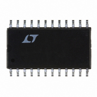
LTC1273BCSW Linear Technology, LTC1273BCSW Datasheet

LTC1273BCSW
Specifications of LTC1273BCSW
Available stocks
Related parts for LTC1273BCSW
LTC1273BCSW Summary of contents
Page 1
... Multiplexed Data Acquisition Systems ■ Audio and Telecom Processing ■ Spectrum Analysis , LT, LTC and LTM are registered trademarks of Linear Technology Corporation. LTBiCMOS is a trademark of Linear Technology Corporation. All other trademarks are the property of their respective owners. U TYPICAL APPLICATIO Single 5V Supply, 300ksps, 12-Bit Sampling A/D Converter ...
Page 2
... Storage Temperature Range ................ – 65°C to 150°C DD Lead Temperature (Soldering, 10 sec)................. 300°C – 0.3V to 12V ORDER PART NUMBER REF LTC1273ACN AGND 3 LTC1273BCN D11 4 D10 5 LTC1273ACSW D9 6 LTC1273BCSW DGND 12 N PACKAGE 24-LEAD PDIP T JMAX T JMAX – 0. ORDER TOP VIEW PART NUMBER V 24 ...
Page 3
U CO VERTER C HARA TERISTICS C temperature range, otherwise specfications are at T PARAMETER CONDITIONS Resolution (No Missing Codes) Integral Linearity Error (Note 7) Commercial Military Differential Linearity Error Commercial Military Offset Error (Note 8) Gain Error Gain Error ...
Page 4
LTC1273 LTC1275/LTC1276 U U DIGITAL I PUTS A D DIGITAL OUTPUTS full operating temperature range, otherwise specfications are at T SYMBOL PARAMETER V High Level Input Voltage IH V Low Level Input Voltage IL I Digital Input Current IN C ...
Page 5
CHARACTERISTICS range, otherwise specfications are SYMBOL PARAMETER t Data Access Time After RD↓ Pulse Width Hold Time 5 t Data Setup Time After BUSY↑ ...
Page 6
LTC1273 LTC1275/LTC1276 CHARACTERISTICS Slow Memory Mode, Parallel Read Timing Diagram CONV BUSY OLD DATA DATA DB11 TO DB0 DB11 TO DB0 t 12 HOLD ...
Page 7
W U TYPICAL PERFOR A Integral Nonlinearity 1.0 0.5 0 –0.5 –1.0 0 512 1024 1536 2048 2560 3072 3584 4096 CODE LTC1273/75/76 • TPC01 ENOBs and S/( Input Frequency ...
Page 8
LTC1273 LTC1275/LTC1276 W U TYPICAL PERFOR A Intermodulation Distortion Plot 300kHz SAMPLE f = 29.37kHz IN1 – 32.446kHz IN2 –40 –60 –80 –100 –120 120 140 100 160 FREQUENCY (kHz) ...
Page 9
(Pin 23): Negative Supply. – 5V for LTC1275/ SS LTC1276. Bypass to AGND with 0.1µF ceramic. NC (Pin 23): No Connection for LTC1273. Table 1. Data Bus Output, CS and ...
Page 10
LTC1273 LTC1275/LTC1276 PPLICATI S I FOR ATIO CONVERSION DETAILS The LTC1273/LTC1275/LTC1276 use a successive ap- proximation algorithm and an internal sample-and-hold circuit to convert an analog signal to a 12-bit parallel or 2-byte output. The ADCs ...
Page 11
PPLICATI S I FOR ATIO Effective Number of Bits The Effective Number of Bits (ENOBs measurement of the resolution of an ADC and is directly related to the S/( the equation: ...
Page 12
LTC1273 LTC1275/LTC1276 PPLICATI S I FOR ATIO Figure 5 shows the IMD performance at a 30kHz input SAMPLE f = 29.37kHz IN1 – 32.446kHz IN2 –40 –60 –80 –100 –120 0 20 ...
Page 13
PPLICATI S I FOR ATIO reference pin. The V pin must be driven to at least REF 2.45V to prevent conflict with the internal reference. The reference should be driven to no more than 4.8V to ...
Page 14
LTC1273 LTC1275/LTC1276 PPLICATI S I FOR ATIO R1 ANALOG 10k + INPUT 10k 10k R4 – 5V 100k R9 R5 20Ω 4.3k FULL SCALE ADJUST R3 100k R6 400Ω Figure 10b. LTC1273 ...
Page 15
PPLICATI S I FOR ATIO ANALOG INPUT CIRCUITRY – error voltage in series with the input signal, attention should be paid to reducing the ground circuit impedances as much as possible. A ...
Page 16
LTC1273 LTC1275/LTC1276 PPLICATI S I FOR ATIO on all three inputs to initiate a conversion. Once initiated it cannot be restarted until the conversion is complete. Converter status is indicated by the BUSY output, and this ...
Page 17
PPLICATI S I FOR ATIO HBEN BUSY t 3 OLD DATA DATA t 12 HOLD TRACK Figure 14. Slow Memory Mode, Two Byte Read Timing Diagram Table ...
Page 18
LTC1273 LTC1275/LTC1276 PPLICATI S I FOR ATIO BUSY DATA HOLD TRACK Figure 15. ROM Mode, Parallel Read Timing Diagram (HBEN = LOW) Table 4. ROM Mode, Parallel Read Data Bus Status Data Outputs D11 ...
Page 19
PPLICATI S I FOR ATIO TMS320C25 Figure 17 shows an interface between the LTC1273 and the TMS320C25. The W/R signal of the DSP initiates a conversion and conversion results are read from the LTC1273 using the ...
Page 20
LTC1273 LTC1275/LTC1276 PPLICATI S I FOR ATIO This is a two byte read instruction which loads the ADC data (address B000) into the HL register pair. During the first read operation, BUSY forces the microprocessor to ...
Page 21
PPLICATI S I FOR ATIO Demodulating a Signal by Undersampling with LTC1275 Figure 23 shows a 455kHz amplitude modulated input undersampled by the LTC1275. With a 227.5kHz sample rate, the converter provides a 100dB noise floor ...
Page 22
LTC1273 LTC1275/LTC1276 PPLICATI S I FOR ATIO 7V 65Ω 1N457 LM134 45.3Ω 1N457 45.3Ω 74HC74 START↑ CLK Q CLR STOP↑ CLK Q CLR 2N2369 2N2369 ...
Page 23
... MOLD FLASH OR PROTRUSIONS SHALL NOT EXCEED .006" (0.15mm) Information furnished by Linear Technology Corporation is believed to be accurate and reliable. However, no responsibility is assumed for its use. Linear Technology Corporation makes no representation that the interconnection of its circuits as described herein will not infringe on existing patent rights. ...
Page 24
... Single Supply, 14mW, 10-Pin MSOP Package 130µA Supply Current, 10ppm/°C, SOT-23 Package 60µA Supply Current, 10ppm/°C, SOT-23 Package 5V Single Supply, 4.25mW, 10-Pin MSOP Package 5V Single Supply, 4.25mW, 10-Pin MSOP Package www.linear.com ● 127356fa LT 0107 REV A • PRINTED IN USA © LINEAR TECHNOLOGY CORPORATION 1993 ...


