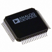
AD9248BSTZ-40 Analog Devices Inc, AD9248BSTZ-40 Datasheet - Page 22

AD9248BSTZ-40
Manufacturer Part Number
AD9248BSTZ-40
Description
IC ADC 14BIT DUAL 40MSPS 64-LQFP
Manufacturer
Analog Devices Inc
Datasheet
1.AD9248BSTZ-20.pdf
(48 pages)
Specifications of AD9248BSTZ-40
Data Interface
Parallel
Number Of Bits
14
Sampling Rate (per Second)
40M
Number Of Converters
2
Power Dissipation (max)
330mW
Voltage Supply Source
Single Supply
Operating Temperature
-40°C ~ 85°C
Mounting Type
Surface Mount
Package / Case
64-LQFP
Resolution (bits)
14bit
Sampling Rate
40MSPS
Input Channel Type
Single Ended
Supply Voltage Range - Analog
2.7V To 3.6V
Supply Current
110mA
Digital Ic Case Style
QFP
Lead Free Status / RoHS Status
Lead free / RoHS Compliant
Available stocks
Company
Part Number
Manufacturer
Quantity
Price
Company:
Part Number:
AD9248BSTZ-40
Manufacturer:
Analog Devices Inc
Quantity:
10 000
Part Number:
AD9248BSTZ-40
Manufacturer:
ADI/亚德诺
Quantity:
20 000
AD9248
AD9248 LQFP EVALUATION BOARD
The evaluation board supports both the AD9238 and AD9248
and has five main sections: clock circuitry, inputs, reference
circuitry, digital control logic, and outputs. A description of
each section follows. Table 8 shows the jumper settings and
notes assumptions in the comment column.
Four supply connections to TB1 are necessary for the evaluation
board: the analog supply of the DUT, the on-board analog
circuitry supply, the digital driver DUT supply, and the on-
board digital circuitry supply. Separate analog and digital
supplies are recommended, and on each supply 3 V is nominal.
Each supply is decoupled on-board, and each IC, including the
DUT, is decoupled locally. All grounds should be tied together.
CLOCK CIRCUITRY
The clock circuitry is designed for a low jitter sine wave source
to be ac-coupled and level shifted before driving the 74VHC04
hex inverter chips (U8 and U9) whose output provides the clock
to the part. The POT (R32 and R31) on the level shifting
circuitry allows the user to vary the duty cycle if desired. The
amplitude of the sine wave must be large enough for the trip
points of the hex inverter and within the supplies to avoid noise
from clipping. To ensure a 50% duty cycle internal to the part,
the AD9248-65 has an on-chip duty cycle stabilizer circuit that
is enabled by putting in Jumper JP11. The duty cycle stabilizer
circuitry should only be used at clock rates above 40 MSPS.
Each channel has its own clock circuitry, but normally both
clock pins are driven by a single 74VHC04, and the solder
Jumper JP24 is used to tie the clock pins together. When the
clock pins are tied together and only one 74VHC04 is being
used, the series termination resistor for the other channel must
be removed (either R54 or R55, depending on which inverter is
being used).
A data capture clock for each channel is created and sent to the
output buffers in order to be used in the data capture system if
needed. Jumper JP25 and Jumper JP26 are used to invert the
data clock, if necessary, and can be used to debug data capture
timing problems.
ANALOG INPUTS
The AD9248 achieves the best performance with a differential
input. The evaluation board has two input options for each
channel, a transformer (XFMR) and an AD8138, both of which
perform single-ended-to-differential conversions. The XFMR
allows for the best high frequency performance, and the
AD8138 is ideal for dc evaluation, low frequency inputs, and
driving an ADC differentially without loading the single-ended
signal.
Rev. B | Page 22 of 48
The common-mode level for both input options is set to
midsupply by a resistor divider off the AVDD supply but can
also be overdriven with an external supply using the (test
points) TP12, TP13 for the AD8138s, and TP14, TP15 for the
XFMRs. For low distortion of full-scale input signals when
using an AD8138, put Jumper JP17 and Jumper JP22 in
Position B and put an external negative supply on the TP10 and
TP11 testpoints.
For best performance, use low jitter input sources and a high
performance band-pass filter after the signal source, before the
evaluation board (see Figure 39). For XFMR inputs, use solder
Jumper JP13 and Jumper JP14 for Channel A, and Jumper JP20
and Jumper JP21 for Channel B. For AD8138 inputs, use solder
Jumper JP15 and Jumper JP16 for Channel A, and Jumper JP18
and Jumper JP19 for Channel B. Remove all solder from the
jumpers not being used.
REFERENCE CIRCUITRY
The evaluation board circuitry allows the user to select a
reference mode through a series of jumpers and provides an
external reference if necessary. Please refer to Table 9 to find the
jumper settings for each reference mode. The external reference
on the board is a simple resistor divider/zener diode circuit
buffered by an AD822 (U4). The POT (R4) can be used to
change the level of the external reference to fine adjust the ADC
full scale.
DIGITAL CONTROL LOGIC
The digital control logic on the evaluation board is a series of
jumpers and pull-down resistors used as digital inputs for the
following pins on the AD9248: the power-down and output
enable bar for each channel, the duty cycle restore circuitry, the
twos complement output mode, the shared reference mode, and
the MUX_SELECT pin. Refer to Table 8 for normal operating
jumper positions.
OUTPUTS
The outputs of the AD9248 (and the data clock discussed
earlier) are buffered by 74VHC541s (U2, U3, U7, U10) to
ensure the correct load on the outputs of the DUT, as well as the
extra drive capability to the next part of the system. The
74VHC541s are latches, but on this evaluation board, they are
wired and function as buffers. Jumper JP30 can be used to tie
the data clocks together if desired. If the data clocks are tied, the
R39 or R40 resistor must be removed, depending on which
clock circuitry is being used.


