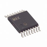
MAX1416EUE+ Maxim Integrated Products, MAX1416EUE+ Datasheet - Page 23

MAX1416EUE+
Manufacturer Part Number
MAX1416EUE+
Description
IC ADC 16BIT DELTA SIGMA 16TSSOP
Manufacturer
Maxim Integrated Products
Datasheet
1.MAX1415EUE.pdf
(36 pages)
Specifications of MAX1416EUE+
Number Of Bits
16
Sampling Rate (per Second)
500
Data Interface
MICROWIRE™, QSPI™, Serial, SPI™
Number Of Converters
1
Power Dissipation (max)
755mW
Voltage Supply Source
Single Supply
Operating Temperature
-45°C ~ 85°C
Mounting Type
Surface Mount
Package / Case
16-TSSOP
Lead Free Status / RoHS Status
Lead free / RoHS Compliant
In internal oscillator mode (INTCLK = 1), set the CLK bit
in the clock register
frequency of 1MHz, or set CLK to 1 for a frequency of
2.4576MHz. The CLKDIV bit is not used in this mode.
The internal clock requires time to stabilize during
power-on reset. This startup time is dependent on the
internal-clock frequency (see the Typical Operating
Characteristics section). The typical startup time for the
internal oscillator is less than 35µs, while the external
oscillator startup time when using a crystal or resonator
is in the order of milliseconds.
The oscillator requires time to stabilize when enabled.
Startup time for the oscillator depends on supply voltage,
temperature, load capacitances, and center frequency.
Depending on the load capacitance, a 1MΩ feedback
resistor across the crystal can reduce the startup time
(Figure 7). The MAX1415/MAX1416 were tested with an
ECS-24-32-1 (2.4576MHz crystal) and an ECS-49-20-1
(4.9152MHz crystal) (see the Typical Operating Char-
acteristics section). When the external oscillator is
enabled, the supply current is typically 67µA with a 3V
supply and 227µA with a 5V supply.
The MAX1415/MAX1416 interface is fully compatible with
SPI-, QSPI-, and MICROWIRE-standard serial interfaces.
The serial interface provides access to seven on-chip
registers. The registers are 8, 16, and 24 bits in size.
Drive CS low to transfer data in and out of the
MAX1415/MAX1416. Clock in data at DIN on the rising
edge of SCLK. Data at DOUT changes on the falling
edge of SCLK and is valid on the rising edge of SCLK.
DIN and DOUT are transferred MSB first. Drive CS high
to force DOUT high impedance and cause the
MAX1415/MAX1416 to ignore any signals on SCLK and
Figure 7. Using a Crystal or Ceramic Oscillator
C
C
L
L
CRYSTAL OR
RESONATOR
CERAMIC
______________________________________________________________________________________
(Table 12) to 0 to operate at a clock
OPTIONAL
Internal Oscillator Mode
1MΩ
Serial Digital Interface
Internal-Clock Startup Time
External Oscillator
CLKIN
CLKOUT
MAX1415
MAX1416
16-Bit, Low-Power, 2-Channel,
DIN. Connect CS low for 3-wire operation. Figures 8
and 9 show the timings for write and read operations,
respectively.
The MAX1415/MAX1416 contain seven internal registers
(Figure 10), which are accessed by the serial interface.
These registers control the various functions of the device
and allow the results to be read. Table 7 lists the address,
power-on default value, and size of each register.
The first of these registers is the communications register.
The 8-bit communications register controls the acquisi-
tion-channel selection, whether the next data transfer is a
read or write operation, and which register is to be
accessed. The second register is the 8-bit setup register,
which controls calibration modes, gain setting,
unipolar/bipolar inputs, and buffered/unbuffered modes.
The third register is the 8-bit clock register, which sets the
digital filter characteristics and the clock control bits. The
fourth register is the 16-bit data register, which holds the
output result. The 24-bit offset and gain registers store the
calibration coefficients for the MAX1415/MAX1416. The 8-
bit test register is used for factory testing only.
Figure 8. Write Timing Diagram
Figure 9. Read Timing Diagram
DRDY
DOUT
SCLK
SCLK
DIN
CS
CS
t
1
t
3
t
Sigma-Delta ADCs
2
t
2
t
9
MSB
MSB
t
10
t
4
t
5
On-Chip Registers
LSB
LSB
t
8
t
6
t
7
t
6
23


