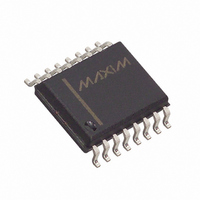
MAX194BEWE+ Maxim Integrated Products, MAX194BEWE+ Datasheet - Page 2

MAX194BEWE+
Manufacturer Part Number
MAX194BEWE+
Description
IC ADC 14BIT 85KSPS 16-SOIC
Manufacturer
Maxim Integrated Products
Datasheet
1.MAX194BEWE.pdf
(24 pages)
Specifications of MAX194BEWE+
Number Of Bits
14
Sampling Rate (per Second)
85k
Data Interface
QSPI™, Serial, SPI™
Number Of Converters
1
Power Dissipation (max)
80mW
Voltage Supply Source
Analog and Digital, Dual ±
Operating Temperature
-40°C ~ 85°C
Mounting Type
Surface Mount
Package / Case
16-SOIC (0.300", 7.50mm Width)
Conversion Rate
85 KSPs
Resolution
14 bit
Maximum Operating Temperature
+ 85 C
Mounting Style
SMD/SMT
Input Voltage
5 V
Minimum Operating Temperature
- 40 C
Lead Free Status / RoHS Status
Lead free / RoHS Compliant
ABSOLUTE MAXIMUM RATINGS
VDDD to DGND .....................................................................+7V
VDDA to AGND......................................................................+7V
VSSD to DGND.........................................................+0.3V to -6V
VSSA to AGND .........................................................+0.3V to -6V
VDDD to VDDA, VSSD to VSSA ..........................................±0.3V
AIN, REF ....................................(VSSA - 0.3V) to (VDDA + 0.3V)
AGND to DGND ..................................................................±0.3V
Digital Inputs to DGND...............................-0.3V, (VDDA + 0.3V)
Digital Outputs to DGND............................-0.3V, (VDDA + 0.3V)
14-Bit, 85ksps ADC with 10µA Shutdown
Stresses beyond those listed under “Absolute Maximum Ratings” may cause permanent damage to the device. These are stress ratings only, and functional
operation of the device at these or any other conditions beyond those indicated in the operational sections of the specifications is not implied. Exposure to
absolute maximum rating conditions for extended periods may affect device reliability.
ELECTRICAL CHARACTERISTICS
(VDDD = VDDA = +5V, VSSD = VSSA = -5V, f
values are at T
2
Resolution
Differential Nonlinearity
ACCURACY (Note 1)
Integral Nonlinearity
Unipolar/Bipolar Offset Error
Unipolar/Bipolar Offset Tempco
Unipolar Full-Scale Error
Bipolar Full-Scale Error
Full-Scale Tempco
Power-Supply Rejection
Ratio (VDDA and VSSA only)
ANALOG INPUT
Input Range
Input Capacitance
DYNAMIC PERFORMANCE (f
Signal-to-Noise plus Distortion
Ratio
Total Harmonic Distortion
(up to the 5th harmonic)
Peak Spurious Noise
Conversion Time
Clock Frequency
(Notes 2, 3)
Serial Clock Frequency
_______________________________________________________________________________________
PARAMETER
A
= +25°C.)
s
= 85kHz, bipolar range AIN = -5V to +5V, 1kHz) (Note 1)
SYMBOL
SINAD
t
f
CONV
RES
DNL
THD
f
SCLK
INL
CLK
CLK
MAX194A
MAX194B
MAX194A, V
MAX194B, V
MAX194A, V
MAX194B, V
MAX194A, V
MAX194B, V
VDDA = 4.75V to 5.25V, V
VSSA = -5.25V to -4.75V, V
Unipolar
Bipolar
Unipolar
Bipolar
16(t
= 1.7MHz, V
CLK
)
REF
REF
REF
REF
REF
REF
REF
CONDITIONS
= 4.75V
= 4.75V
= 4.75V
= 4.75V
= 4.75V
= 4.75V
= +5V, T
Continuous Power Dissipation (T
Operating Temperature Ranges
Storage Temperature Range .............................-65°C to +160°C
Lead Temperature (soldering, 10sec) .............................+300°C
Plastic DIP (derate 10.53mW/°C above +70°C) ............842mW
Wide SO (derate 9.52mW/°C above +70°C)..................762mW
Ceramic SB (derate 10.53mW/°C above +70°C)...........842mW
MAX194_C_E ........................................................0°C to +70°C
MAX194_E_E .....................................................-40°C to +85°C
MAX194_MDE..................................................-55°C to +125°C
REF
REF
A
= T
= 4.75V
= 4.75V
MIN
to T
MAX
, unless otherwise noted. Typical
-V
MIN
9.4
14
65
65
82
REF
0
A
= +70°C)
TYP
250
125
0.4
0.1
MAX
V
V
±1⁄2
-90
-90
1.7
±1
±1
±1
±2
±1
±2
±2
±4
REF
REF
5
ppm/°C
ppm/°C
UNITS
MHz
MHz
LSB
LSB
LSB
LSB
LSB
Bits
dB
pF
dB
dB
dB
µs
V


