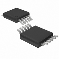
LTC2433-1IMS#TRPBF Linear Technology, LTC2433-1IMS#TRPBF Datasheet - Page 23

LTC2433-1IMS#TRPBF
Manufacturer Part Number
LTC2433-1IMS#TRPBF
Description
IC ADC DIFF 16BIT 3WIRE 10-MSOP
Manufacturer
Linear Technology
Datasheet
1.LTC2433-1CMS.pdf
(28 pages)
Specifications of LTC2433-1IMS#TRPBF
Number Of Bits
16
Sampling Rate (per Second)
6.8
Data Interface
MICROWIRE™, Serial, SPI™
Number Of Converters
2
Power Dissipation (max)
1mW
Voltage Supply Source
Single Supply
Operating Temperature
-40°C ~ 85°C
Mounting Type
Surface Mount
Package / Case
10-TFSOP, 10-MSOP (0.118", 3.00mm Width)
Lead Free Status / RoHS Status
Lead free / RoHS Compliant
Available stocks
Company
Part Number
Manufacturer
Quantity
Price
Larger values of reference capacitors (C
be required as reference filters in certain configurations.
Such capacitors will average the reference sampling charge
and the external source resistance will see a quasi con-
stant reference differential impedance. When F
(internal oscillator and 50Hz/60Hz notch), the typical
differential reference resistance is 4.2M which will gen-
erate a gain error of approximately 1LSB full scale for each
120 of source resistance driving REF
is driven by an external oscillator with a frequency f
(external conversion clock operation), the typical differen-
tial reference resistance is 0.60 • 10
ohm of source resistance drving REF
in 5.1 • 10
APPLICATIO S I FOR ATIO
Figure 21. +FS Error vs R
Figure 19. +FS Error vs R
–8
–10
–5
• f
–1
–2
–3
0
0
0
EOSC
1
C
V
REF
REF
IN
IN
F
T
V
REF
REF
IN
IN
F
T
O
REF
CC
A
100
O
CC
A
+
–
+
–
= GND
= 25 C
= GND
= 25 C
+
–
= 3.75V
= 1.25V
= 5V
+
= 3.75V
–
= 1.25V
= 5V
= 10 F
LSB gain error at full scale. The effect
= 5V
= GND
U
200
= 5V
= GND
10
C
300
REF
SOURCE
C
C
REF
SOURCE
REF
C
= 0.001 F
REF
400
C
R
U
100
R
= 100pF
REF
SOURCE
= 0.01 F
SOURCE
= 0pF
500
= 0.1 F
at REF
C
at REF
REF
600
( )
( )
1k
= 1 F
C
700
+
W
REF
+
and REF
12
+
800
or REF
= 0.01 F
+
10k
or REF
/f
REF
or REF
EOSC
900
24331 F21
24331 F19
> 0.01 F) may
1000
–
–
100k
(Small C
(Large C
–
–
U
. When F
will result
O
and each
= LOW
EOSC
IN
REF
)
)
O
of the source resistance on the two reference pins is
additive with respect to this gain error. The typical +FS and
–FS errors for various combinations of source resistance
seen by the REF
C
21 and 22.
In addition to this gain error, the converter INL perfor-
mance is degraded by the reference source impedance.
When F
every 1000 of source resistance driving REF
translates into about 1LSB additional INL error. When F
is driven by an external oscillator with a frequency f
every 1000 of source resistance driving REF
Figure 22. –FS Error vs R
REF
Figure 20. –FS Error vs R
connected to these pins are shown in Figures 19, 20,
O
= LOW (internal oscillator and 50Hz/60Hz notch),
10
3
2
1
0
5
0
1
0
+
V
REF
REF
IN
IN
F
T
V
REF
REF
IN
IN
F
T
O
O
A
A
CC
CC
and REF
100
+
+
–
–
= GND
= 25 C
= GND
= 25 C
+
–
= 1.25V
+
–
= 1.25V
= 3.75V
= 5V
= 3.75V
= 5V
= 5V
= 5V
= GND
= GND
200
10
C
C
REF
REF
C
SOURCE
300
REF
SOURCE
= 0.001 F
C
= 0.01 F
–
REF
= 100pF
100
R
400
R
pins and external capacitance
SOURCE
SOURCE
= 0pF
C
REF
C
500
at REF
REF
at REF
= 1 F
600
( )
( )
= 0.01 F
1k
C
REF
+
700
C
LTC2433-1
+
REF
and REF
= 10 F
or REF
800
10k
= 0.1 F
900
24331 F20
24331 F22
–
–
1000
100k
(Small C
(Large C
+
+
or REF
or REF
23
EOSC
24331fa
IN
REF
)
)
O
–
–
,


