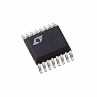
LTC1863CGN Linear Technology, LTC1863CGN Datasheet - Page 7

LTC1863CGN
Manufacturer Part Number
LTC1863CGN
Description
IC ADC 12BIT 8CH 200KSPS 16SSOP
Manufacturer
Linear Technology
Datasheet
1.LTC1867CGNPBF.pdf
(16 pages)
Specifications of LTC1863CGN
Number Of Bits
12
Sampling Rate (per Second)
200k
Data Interface
MICROWIRE™, Serial, SPI™
Number Of Converters
1
Power Dissipation (max)
9mW
Voltage Supply Source
Single Supply
Operating Temperature
0°C ~ 70°C
Mounting Type
Surface Mount
Package / Case
16-SSOP (0.150", 3.90mm Width)
Lead Free Status / RoHS Status
Contains lead / RoHS non-compliant
Available stocks
Company
Part Number
Manufacturer
Quantity
Price
Company:
Part Number:
LTC1863CGN
Manufacturer:
LT
Quantity:
10 000
Part Number:
LTC1863CGN
Manufacturer:
LINEAR/凌特
Quantity:
20 000
Part Number:
LTC1863CGN#PBF
Manufacturer:
LINEAR/凌特
Quantity:
20 000
PIN FUNCTIONS
CHO-CH7/COM (Pins 1-8): Analog Input Pins. Analog
inputs must be free of noise with respect to GND. CH7/COM
can be either a separate channel or the common minus
input for the other channels.
REFCOMP (Pin 9): Reference Buffer Output Pin. Bypass
to GND with 10μF tantalum capacitor in parallel with
0.1μF ceramic capacitor (4.096V Nominal). To overdrive
REFCOMP, tie V
V
be used as an external reference buffer input for improved
accuracy and drift. Bypass to GND with 2.2μF tantalum
capacitor in parallel with 0.1μF ceramic capacitor.
CS/CONV (Pin 11): This input provides the dual function
of initiating conversions on the ADC and also frames the
serial data transfer.
TYPICAL CONNECTION DIAGRAM
TEST CIRCUITS
REF
(Pin 10): 2.5V Reference Output. This pin can also
(A) Hi-Z TO V OH AND V OL TO V OH
DN
Load Circuits for Access Timing
REF
3k
to GND.
C
L
(B) Hi-Z TO V OL AND V OH TO V OL
SINGLE-ENDED
DIFFERENTIAL
DN
±2.048V
INPUTS
4.096V
INPUT
5V
–
+
+
3k
C
L
CH0
CH1
CH2
CH3
CH4
CH5
CH6
CH7/COM
18637 TC01
LTC1863/
LTC1867
REFCOMP
CS/CONV
V
GND
SDO
SCK
SCK (Pin 12): Shift Clock. This clock synchronizes the
serial data transfer.
SDO (Pin 13): Digital Data Output. The A/D conversion
result is shifted out of this output. Straight binary format
for unipolar mode and two’s complement format for
bipolar mode.
SDI (Pin 14): Digital Data Input Pin. The A/D confi guration
word is shifted into this input.
GND (Pin 15): Analog and Digital GND.
V
GND with 10μF tantalum capacitor in parallel with 0.1μF
ceramic capacitor.
V
SDI
REF
DD
DD
(Pin 16): Analog and Digital Power Supply. Bypass to
DIGITAL
I/O
10μF
DN
4.096V
5V
Load Circuits for Output Float Delay
(A) V OH TO Hi-Z
3k
LTC1863/LTC1867
18637 TCD
2.2μF
2.5V
C
L
DN
(B) V OL TO Hi-Z
5V
3k
18637 TC02
C
L
18637fa
7


