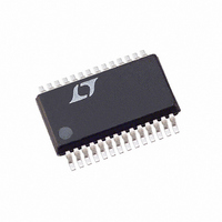
LTC2424IG Linear Technology, LTC2424IG Datasheet - Page 14

LTC2424IG
Manufacturer Part Number
LTC2424IG
Description
IC ADC 20BIT 4CH MICROPWR 28SSOP
Manufacturer
Linear Technology
Datasheet
1.LTC2424CGPBF.pdf
(36 pages)
Specifications of LTC2424IG
Number Of Bits
20
Sampling Rate (per Second)
7.5
Data Interface
MICROWIRE™, Serial, SPI™
Number Of Converters
1
Power Dissipation (max)
1mW
Voltage Supply Source
Single Supply
Operating Temperature
-40°C ~ 85°C
Mounting Type
Surface Mount
Package / Case
28-SSOP (0.200", 5.30mm Width)
Lead Free Status / RoHS Status
Contains lead / RoHS non-compliant
Available stocks
Company
Part Number
Manufacturer
Quantity
Price
Part Number:
LTC2424IG#PBF
Manufacturer:
LINEAR/凌特
Quantity:
20 000
Part Number:
LTC2424IG#TRPBF
Manufacturer:
LINEAR/凌特
Quantity:
20 000
APPLICATIONS
LTC2424/LTC2428
As long as the voltage on the V
the – 0.3V to (V
range, a conversion result is generated for any input value
from – 0.125 • V
greater than 1.125 • V
to the value corresponding to 1.125 • V
voltages below – 0.125 • V
clamped to the value corresponding to – 0.125 • V
14
Table 2. LTC2424/LTC2428 Output Data Format
Input Voltage
V
9/8 • V
V
V
3/4V
3/4V
1/2V
1/2V
1/4V
1/4V
0
–1LSB
–1/8 • V
V
*The sign bit changes state during the 0 code.
IN
REF
REF
+
IN
/0
CSMUX/CSADC
> 9/8 • V
< –1/8 • V
–
REF
REF
REF
REF
REF
REF
+ 1LSB
REF
REF
SCK/CLK
+ 1LSB
+ 1LSB
+ 1LSB
SDO
REF
D
REF
IN
CC
REF
+ 0.3V) absolute maximum operating
EN
U
REF
to 1.125 • V
Bit 23
, the conversion result is clamped
EOC
D2
INFORMATION
0
0
0
0
0
0
0
0
0
0
0
0
0
0
U
REF
Hi-Z
D1
IN
, the conversion result is
Bit 22
DMY
pin is maintained within
REF
0
0
0
0
0
0
0
0
0
0
0
0
0
0
W
D0
. For input voltages
Figure 4. Typical Data Input/Output Timing
Bit 21
1/0*
SIG
1
1
1
1
1
1
1
1
1
1
0
0
0
REF
EOC
BIT 23
. For input
U
Bit 20
BIT 22
EXR
“0”
1
1
1
0
0
0
0
0
0
0
0
1
1
1
REF
.
SIG
Bit 19
MSB
0
0
0
1
1
1
1
0
0
0
0
1
1
1
EXT
Channel Selection
Typically, CSADC and CSMUX are tied together or CSADC
is inverted and drives CSMUX. SCK and CLK are tied
together and driven with a common clock signal. During
channel selection, CSMUX is HIGH. Data is shifted into the
D
shows the bit combinations for channel selection. In order
to enable the multiplexer output, CSMUX must be pulled
IN
Bit 18
pin on the rising edge of CLK, see Figure 4. Table 3
MSB
0
0
0
1
1
0
0
1
1
0
0
1
1
1
DON’T CARE
Bit 17
0
0
0
1
0
1
0
1
0
1
0
1
1
1
LSB
BIT 0
Bit 16
1
1
0
1
0
1
0
1
0
1
0
1
0
0
Bit 15
1
1
0
1
0
1
0
1
0
1
0
1
0
0
t
Hi-Z
CONV
…
...
...
...
...
...
...
...
...
...
...
...
...
...
...
24248 F04
Bit 0
LSB
1
1
0
1
0
1
0
1
0
1
0
1
0
0


