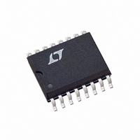
LTC1594IS#TR Linear Technology, LTC1594IS#TR Datasheet

LTC1594IS#TR
Specifications of LTC1594IS#TR
Available stocks
Related parts for LTC1594IS#TR
LTC1594IS#TR Summary of contents
Page 1
... LT, LTC and LTM are registered trademarks of Linear Technology Corporation. All other trademarks are the property of their respective owners. 5V ...
Page 2
LTC1594/LTC1598 ABSOLUTE AXI U RATI GS (Notes 1, 2) Supply Voltage ( GND ................................... 12V CC Voltage Analog Reference .................... – 0. Analog Inputs .......................... – 0. Digital Inputs .........................................– 0.3V ...
Page 3
CONVERTER AND MULTIPLEXER CHARACTERISTICS apply over the full operating temperature range, otherwise specifications are at T PARAMETER CONDITIONS Resolution (No Missing Codes) Integral Linearity Error (Note 6) Differential Linearity Error Offset Error Gain Error REF Input Range ...
Page 4
LTC1594/LTC1598 AC CHARACTERISTICS otherwise specifications are 25°C. (Note 5) A SYMBOL PARAMETER t Analog Input Sample Time SMPL f Maximum Sampling Frequency SMPL(MAX) t Conversion Time CONV t Delay Time, CLK↓ Data Valid dDO OUT ...
Page 5
W U TYPICAL PERFORMANCE CHARACTERISTICS Change in Offset vs Reference Voltage 3 25° 2 320kHz CLK f = 16.8kHz SMPL 2.0 1.5 1.0 0.5 0 3.5 4.0 1.0 1.5 2.0 2.5 ...
Page 6
LTC1594/LTC1598 W U TYPICAL PERFORMANCE CHARACTERISTICS Attenuation vs Input Frequency 25° REF 16.8kHz SMPL 100 1 10 100 1000 ...
Page 7
PIN FUNCTIONS LTC1594 CH0 (Pin 1): Analog Multiplexer Input. CH1 (Pin 2): Analog Multiplexer Input. CH2 (Pin 3): Analog Multiplexer Input. CH3 (Pin 4): Analog Multiplexer Input. ADCIN (Pin 5): ADC Input. This input is the positive ...
Page 8
LTC1594/LTC1598 PIN FUNCTIONS V (Pin 15): Power Supply Voltage. This pin provides CC power to the A/D Converter. It must be bypassed directly to the analog ground plane. V (Pin 16): Reference Input. The reference input de- ...
Page 9
TEST CIRCUITS Voltage Waveforms for D Delay Times, t OUT CSMUX = CSADC = CS CLK DON‘T CARE OUT B11 B10 MPU ...
Page 10
LTC1594/LTC1598 U U APPLICATIONS INFORMATION OVERVIEW The LTC1594/LTC1598 are micropower, 12-bit sampling A/D converters that feature a 4- and 8-channel multi- plexer respectively. They typically draw only 320μA of supply current when sampling at 16.8kHz. Supply cur- rent drops linearly ...
Page 11
U U APPLICATIONS INFORMATION CSMUX = CSADC = CS CLK Hi-Z D OUT CH0 TO CH7 ADCIN = MUXOUT COM = GND Figure 2. LTC1594/LTC1598 Operating Sequence Example: All Channels Off Data Transfer The CLK synchronizes ...
Page 12
LTC1594/LTC1598 U U APPLICATIONS INFORMATION after a delay all the channels are switched off to OFF ensure a break-before-make interval. After this interval, the selected channel is switched on allowing signal transmission. The selected channel remains on ...
Page 13
U U APPLICATIONS INFORMATION Operation with D and D Tied Together IN OUT The LTC1594/LTC1598 can be operated with D D tied together. This eliminates one of the lines OUT required to communicate to the microprocessor (MPU). Data is transmitted ...
Page 14
LTC1594/LTC1598 U U APPLICATIONS INFORMATION CSADC CSMUX t suCS CLK NULL BIT D OUT SMPL CH0 TO CH7 t ON ADCIN = MUXOUT COM = GND Figure 5. ...
Page 15
U U APPLICATIONS INFORMATION BOARD LAYOUT CONSIDERATIONS Grounding and Bypassing The LTC1594/LTC1598 are easy to use if some care is taken. They should be used with an analog ground plane and single point grounding techniques. The GND pin should be ...
Page 16
LTC1594/LTC1598 U U APPLICATIONS INFORMATION edge, the S & H goes into hold mode and the conversion begins. The voltage on the “COM” input must remain constant and be free of noise and ripple throughout the conversion time. Otherwise, the ...
Page 17
U U APPLICATIONS INFORMATION Input Leakage Current Input leakage currents can also create errors if the source resistance gets too large. For instance, the maximum input leakage specification of 200nA (at 85°C) flowing through a source resistance of 1.2k will ...
Page 18
LTC1594/LTC1598 U U APPLICATIONS INFORMATION Conversion Speed with Reduced V With reduced reference voltages, the LSB step size is reduced and the LTC1594/LTC1598 internal comparator overdrive is reduced. Therefore, it may be necessary to reduce the maximum CLK frequency when ...
Page 19
U U APPLICATIONS INFORMATION specification in the Dynamic Accuracy table includes the 2nd through 5th harmonics. With a 7kHz input signal, the LTC1594/LTC1598 have typical THD of 80dB with V Intermodulation Distortion If the ADC input signal consists of more ...
Page 20
LTC1594/LTC1598 U TYPICAL APPLICATIONS LDA #$52 Configuration data for serial peripheral control register (Interrupts disabled, output enabled, master, Norm = Clk/16) STA $0A Load configuration data into location $0A (SPCR) LDA #$FF Configuration data for I/O ...
Page 21
U TYPICAL APPLICATIONS MULTICHANNEL A/D USES A SINGLE ANTIALIASING FILTER This circuit demonstrates how the LTC1598’s indepen- dent analog multiplexer can simplify design of a 12-bit data acquisition system. All eight channels are MUXed into a single 1kHz, 4th order ...
Page 22
LTC1594/LTC1598 U TYPICAL APPLICATIONS Using MUXOUT/ADCIN Loop as PGA This figure shows the LTC1598’s MUXOUT/ADCIN loop and an LT1368 being used to create a single channel PGA with eight noninverting gains. Combined with the LTC1391, the system can expand to ...
Page 23
... MOLD FLASH OR PROTRUSIONS SHALL NOT EXCEED .006" (0.15mm) Information furnished by Linear Technology Corporation is believed to be accurate and reliable. However, no responsibility is assumed for its use. Linear Technology Corporation makes no represen- tation that the interconnection of its circuits as described herein will not infringe on existing patent rights. ...
Page 24
... Low Power, Small Size, Low Cost Low Power, Small Size, Low Cost www.linear.com ● 15, 19 1μ REF CC 10 CSADC 6 CSMUX 5, 14 CLK OUT 12 NC LTC1598 1594/98 TA07 , CLK, Sample-and-Hold REF , CLK, Sample-and-Hold REF LT 0507 REV B • PRINTED IN USA © LINEAR TECHNOLOGY CORPORATION 1996 15948fb ...


