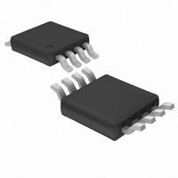
LTC1864LACMS8#TRPBF Linear Technology, LTC1864LACMS8#TRPBF Datasheet - Page 4

LTC1864LACMS8#TRPBF
Manufacturer Part Number
LTC1864LACMS8#TRPBF
Description
IC ADC 16-BIT 1CH 150KSPS 8-MSOP
Manufacturer
Linear Technology
Datasheet
1.LTC1865LCMSPBF.pdf
(16 pages)
Specifications of LTC1864LACMS8#TRPBF
Number Of Bits
16
Sampling Rate (per Second)
150k
Data Interface
MICROWIRE™, Serial, SPI™
Number Of Converters
1
Power Dissipation (max)
400mW
Voltage Supply Source
Single Supply
Operating Temperature
0°C ~ 70°C
Mounting Type
Surface Mount
Package / Case
8-TSSOP, 8-MSOP (0.118", 3.00mm Width)
Lead Free Status / RoHS Status
Lead free / RoHS Compliant
Available stocks
Company
Part Number
Manufacturer
Quantity
Price
LTC1864L/LTC1865L
RECO
full operating temperature range, otherwise specifications are T
SYMBOL PARAMETER
V
f
t
t
t
t
t
t
t
t
t
t
range, otherwise specifications are T
Conditions, unless otherwise noted.
TI I G CHARACTERISTICS
SYMBOL
t
f
t
t
t
t
t
t
Note 1: Absolute Maximum Ratings are those values beyond which the life
of a device may be impaired.
Note 2: All voltage values are with respect to GND.
Note 3: Integral nonlinearity is defined as deviation of a code from a
straight line passing through the actual endpoints of the transfer curve.
The deviation is measured from the center of the quantization band.
4
SCK
CYC
SMPL
suCONV
hDI
suDI
WHCLK
WLCLK
WHCONV
WLCONV
hCONV
CONV
SMPL(MAX)
dDO
dis
en
hDO
r
f
CC
W
U
Supply Voltage
Clock Frequency
Total Cycle Time
Analog Input Sampling Time (Note 5)
Setup Time CONV↓ Before First SCK↑
(See Figure 1)
Hold Time SDI After SCK↑
Setup Time SDI Stable Before SCK↑
SCK High Time
SCK Low Time
CONV High Time Between Data
Transfer Cycles
CONV Low Time During Data Transfer
Hold Time CONV Low After Last SCK↑
W W
PARAMETER
Conversion Time (See Figure 1)
Maximum Sampling Frequency
Delay Time, SCK↓ to SDO Data Valid
Delay Time, CONV↑ to SDO Hi-Z
Delay Time, CONV↓ to SDO Enabled
Time Output Data Remains
Valid After SCK↓
SDO Rise Time
SDO Fall Time
E DED OPERATI G CO DITIO S
U
A
= 25°C. V
CC
U
CONDITIONS
LTC1864L
LTC1865L
LTC1865L
LTC1865L
f
f
= 2.7V, V
CONDITIONS
C
C
C
C
C
SCK
SCK
The
LOAD
LOAD
LOAD
LOAD
LOAD
= f
= f
●
= 20pF
= 20pF
= 20pF
= 20pF
= 20pF
SCK(MAX)
SCK(MAX)
denotes specifications which apply over the full operating temperature
REF
U
A
= 2.5V, f
= 25°C.
Note 4: Channel leakage current is measured while the part is in sample
mode.
Note 5: Assumes f
not have to be clocked during this time if the SDO data word is not
desired. In the case of the LTC1865L a minimum of 2 clocks are required
on the SCK input after CONV falls to configure the MUX during this time.
SCK
U
= f
SCK(MAX)
The
SCK
●
as defined in Recommended Operating
= f
denotes specifications which apply over the
SCK(MAX)
●
●
●
●
●
●
●
In the case of the LTC1864L SCK does
16 • SCK + t
t
45%
45%
MIN
CONV
MIN
150
2.7
DC
16
14
60
30
30
16
26
5
LTC1864L/LTC1865L
LTC1864L/LTC1865L
TYP
CONV
TYP
3.7
45
55
35
15
25
12
MAX
MAX
4.66
3.6
120
120
sn18645L 18645Lfs
55
60
8
UNITS
1/f
1/f
UNITS
MHz
SCK
SCK
SCK
SCK
SCK
kHz
µs
ns
ns
ns
µs
ns
µs
ns
ns
ns
ns
ns
ns
ns
V


