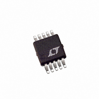
LTC1403AIMSE Linear Technology, LTC1403AIMSE Datasheet - Page 11

LTC1403AIMSE
Manufacturer Part Number
LTC1403AIMSE
Description
IC ADC 14BIT 2.8MSPS DIFF 10MSOP
Manufacturer
Linear Technology
Datasheet
1.LTC1403CMSEPBF.pdf
(20 pages)
Specifications of LTC1403AIMSE
Number Of Bits
14
Sampling Rate (per Second)
2.8M
Data Interface
Serial, SPI™
Number Of Converters
1
Power Dissipation (max)
12mW
Voltage Supply Source
Single Supply
Operating Temperature
-40°C ~ 125°C
Mounting Type
Surface Mount
Package / Case
10-TFSOP, 10-MSOP (0.118", 3.00mm Width) Exposed Pad
Lead Free Status / RoHS Status
Contains lead / RoHS non-compliant
Available stocks
Company
Part Number
Manufacturer
Quantity
Price
Company:
Part Number:
LTC1403AIMSE
Manufacturer:
LT
Quantity:
10 000
Part Number:
LTC1403AIMSE
Manufacturer:
LT
Quantity:
20 000
Part Number:
LTC1403AIMSE#PBF
Manufacturer:
LT/凌特
Quantity:
20 000
Company:
Part Number:
LTC1403AIMSE-1
Manufacturer:
LT
Quantity:
10 000
Company:
Part Number:
LTC1403AIMSE-1#PBF
Manufacturer:
LT
Quantity:
1 000
Part Number:
LTC1403AIMSE-1#PBF
Manufacturer:
LINEAR/凌特
Quantity:
20 000
Company:
Part Number:
LTC1403AIMSE-1#TRPBF
Manufacturer:
LT
Quantity:
1 000
INPUT SPAN VERSUS REFERENCE VOLTAGE
The differential input range has a unipolar voltage span that
equals the difference between the voltage at the reference
buffer output V
(Exposed Pad Ground). The differential input range of
the ADC is 0V to 2.5V when using the internal reference.
The internal ADC is referenced to these two nodes. This
relationship also holds true with an external reference.
DIFFERENTIAL INPUTS
The LTC1403/LTC1403A has a unique differential sample-
and-hold circuit that allows inputs from ground to V
The ADC will always convert the unipolar difference of
A
APPLICATIONS INFORMATION
IN
+
– A
IN
–
–100
–120
, independent of the common mode voltage
–20
–40
–60
–80
0
100
REF
at Pin 3, and the voltage at the ground
1k
CMRR vs Frequency
10k
FREQUENCY (Hz)
Figure 3
100k
1M
10M 100M
1403A F03
DD
.
at the inputs. The common mode rejection holds up at
extremely high frequencies, see Figure 3. The only require-
ment is that both inputs not go below ground or exceed
V
nonlinearity errors (DNL) are largely independent of the
common mode voltage. However, the offset error will vary.
The change in offset error is typically less than 0.1% of
the common mode voltage.
Figure 4 shows the ideal input/output characteristics for
the LTC1403/LTC1403A. The code transitions occur mid-
way between successive integer LSB values (i.e., 0.5LSB,
1.5LSB, 2.5LSB, FS – 1.5LSB). The output code is natural
binary with 1LSB = 2.5V/16384 = 153μV for the LTC1403A,
and 1LSB = 2.5V/4096 = 610μV for the LTC1403. The
LTC1403A has 1LSB RMS of random white noise.
DD
. Integral nonlinearity errors (INL) and differential
111...111
111...110
111...101
000...010
000...001
000...000
0
LTC1403/LTC1403A
LTC1403/LTC1403A Transfer
Figure 4
INPUT VOLTAGE (V)
Characteristic
FS – 1LSB
1403A F05
11
1403fb


