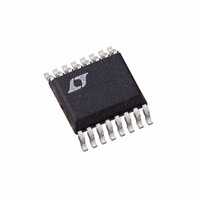
LTC1417ACGN Linear Technology, LTC1417ACGN Datasheet - Page 17

LTC1417ACGN
Manufacturer Part Number
LTC1417ACGN
Description
IC A/D CONV 14BIT SAMPLNG 16SSOP
Manufacturer
Linear Technology
Datasheet
1.LTC1417CGNPBF.pdf
(32 pages)
Specifications of LTC1417ACGN
Number Of Bits
14
Sampling Rate (per Second)
400k
Data Interface
MICROWIRE™, Serial, SPI™
Number Of Converters
1
Power Dissipation (max)
27.5mW Unipolar; 44mW Bipolar
Voltage Supply Source
Dual ±
Operating Temperature
0°C ~ 70°C
Mounting Type
Surface Mount
Package / Case
16-SSOP (0.150", 3.90mm Width)
Lead Free Status / RoHS Status
Contains lead / RoHS non-compliant
Available stocks
Company
Part Number
Manufacturer
Quantity
Price
Company:
Part Number:
LTC1417ACGN
Manufacturer:
LT
Quantity:
10 000
Part Number:
LTC1417ACGN
Manufacturer:
LTNEAR
Quantity:
20 000
Company:
Part Number:
LTC1417ACGN#PBF
Manufacturer:
CYPRESS
Quantity:
120
Part Number:
LTC1417ACGN#PBF
Manufacturer:
LINEAR/凌特
Quantity:
20 000
Company:
Part Number:
LTC1417ACGN#TRPBF
Manufacturer:
LT
Quantity:
450
APPLICATIONS
DIGITAL INTERFACE
The LTC1417 operates in serial mode. The RD control input
is common to all peripheral memory interfacing. Only four
digital interface lines are required, SCLK, CONVST,
EXTCLKIN and D
be an external input or supplied by the LTC1417’s internal
clock.
Internal Clock
The ADC has an internal clock. Either the internal clock or
an external clock may be used as the conversion clock (see
Figure 15). The internal clock is factory trimmed to achieve
a typical conversion time of 1.8 s, and a maximum con-
version time over the full operating temperature range of
2.5 s. No external adjustments are required, and with the
guaranteed maximum acquisition time of 0.5 s, through-
put performance of 400ksps is assured.
Conversion Control
Conversion start is controlled by the signal applied to the
CONVST input. A falling edge on the signal applied to the
CONVST pin starts a conversion. Once initiated, it cannot
be restarted until the conversion is complete. Converter
OUT
SAR
U
. SCLK, the serial data shift clock can
INFORMATION
U
DATA
EOC
14
IN
16 CONVERSION CLOCK CYCLES
CLOCK
INPUT
W
REGISTER
SHIFT
Figure 15. Functional Block Diagram
U
DATA
OUT
BUFFER
THREE
STATE
DETECTOR
INTERNAL
CLOCK
CLOCK
status is indicated by the BUSY output. BUSY is low during
a conversion.
Data Output
Output will be active when RD is low. A high RD will three-
state the ouput. In unipolar mode (V
be in straight binary format (corresponding to the unipolar
input range). In bipolar mode (V
in two’s complement format (corresponding to the bipolar
input range).
Serial Output Mode
Conversions are started by a falling CONVST edge. After a
conversion is completed and the output shift register has
been updated, BUSY will go high and valid data will be
available on D
either before the next conversion starts or it can be clocked
out during the next conversion. To enable the serial data
output buffer and shift clock, RD must be low.
Figure 15 shows a function block diagram of the LTC1417.
There are two pieces to this circuitry: the conversion clock
selection circuit (EXTCLKIN and CLKOUT) and the serial
port (SCLK, D
BUFFER
THREE
STATE
OUT
OUT
and RD).
(Pin 9). This data can be clocked out
• • •
• • •
SS
7
12
9
8
6
14
= – 5V), the data will be
SS
SCLK
RD
D
CLKOUT
EXTCLKIN
BUSY
1417 F15
OUT
= 0V), the data will
LTC1417
sn1417 1417fas
17


