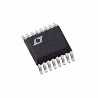
LTC1867ACGN Linear Technology, LTC1867ACGN Datasheet - Page 3

LTC1867ACGN
Manufacturer Part Number
LTC1867ACGN
Description
IC ADC 16BIT 8CH 200KSPS 16SSOP
Manufacturer
Linear Technology
Datasheet
1.LTC1867CGNPBF.pdf
(16 pages)
Specifications of LTC1867ACGN
Number Of Bits
16
Sampling Rate (per Second)
200k
Data Interface
MICROWIRE™, Serial, SPI™
Number Of Converters
1
Power Dissipation (max)
9mW
Voltage Supply Source
Single Supply
Operating Temperature
0°C ~ 70°C
Mounting Type
Surface Mount
Package / Case
16-SSOP (0.150", 3.90mm Width)
Lead Free Status / RoHS Status
Contains lead / RoHS non-compliant
Available stocks
Company
Part Number
Manufacturer
Quantity
Price
Company:
Part Number:
LTC1867ACGN
Manufacturer:
LT
Quantity:
10 000
Part Number:
LTC1867ACGN
Manufacturer:
LINEAR/凌特
Quantity:
20 000
Company:
Part Number:
LTC1867ACGN#PBF
Manufacturer:
LT
Quantity:
1 000
Company:
Part Number:
LTC1867ACGN#TRPBF
Manufacturer:
LT
Quantity:
1 000
CONVERTER CHARACTERISTICS
temperature range, otherwise specifi cations are at T
PARAMETER
Gain Error Match
Gain Error Tempco
Power Supply Sensitivity
DYNAMIC ACCURACY
SYMBOL PARAMETER
SNR
S/(N+D)
THD
ANALOG INPUT
specifi cations are at T
SYMBOL
C
t
INTERNAL REFERENCE CHARACTERISTICS
DIGITAL INPUTS AND DIGITAL OUTPUTS
full operating temperature range, otherwise specifi cations are at T
SYMBOL
V
V
I
IN
ACQ
PARAMETER
V
V
V
V
REFCOMP Output Voltage
IN
IH
IL
REF
REF
REF
REF
Output Voltage
Output Tempco
Line Regulation
Output Resistance
Signal-to-Noise Ratio
Signal-to-(Noise + Distortion) Ratio 1kHz Input Signal
Total Harmonic Distortion
Peak Harmonic or Spurious Noise
Channel-to-Channel Isolation
Full Power Bandwidth
PARAMETER
Analog Input Range
Analog Input Capacitance for CH0 to
CH7/COM
Sample-and-Hold Acquisition Time
Input Leakage Current
PARAMETER
High Level Input Voltage
Low Level Input Voltage
Digital Input Current
A
= 25°C. (Note 5)
CONDITIONS
Internal Reference
External Reference
V
DD
= 4.75V – 5.25V
The
l
⏐I
CONDITIONS
I
I
4.75V ≤ V
I
denotes the specifi cations which apply over the full operating temperature range, otherwise
OUT
OUT
OUT
OUT
= 0
= 0
= 0
(Note 5)
⏐ ≤0.1mA
CONDITIONS
1kHz Input Signal
1kHz Input Signal, Up to 5th Harmonic
1kHz Input Signal
100kHz Input Signal
–3dB Point
DD
≤ 5.25V
CONDITIONS
Unipolar Mode (Note 9)
Bipolar Mode
Between Conversions (Sample Mode)
During Conversions (Hold Mode)
On Channels, CHX = 0V or V
CONDITIONS
V
V
V
IN
DD
DD
A
= 0V to V
= 5.25V
= 4.75V
= 25°C. With external reference (Notes 5, 6)
The
MIN
DD
l
LTC1863
denotes the specifi cations which apply over the full operating
A
±2.7
TYP
±15
±1
= 25°C. (Note 5)
MAX
DD
±1
The
(Note 5)
MIN
MIN
l
denotes the specifi cations which apply over the
LTC1867
LTC1863
–94.5
–94.5
±2.7
–100
TYP
73.6
73.5
1.25
TYP
±15
±5
l
l
l
l
l
l
l
LTC1863/LTC1867
MAX
LTC1863/LTC1867/LTC1867A
LTC1863/LTC1867/LTC1867A
LTC1863/LTC1867/LTC1867A
MAX
MIN
2.48
±4
MIN
MIN
1.5
2.4
MIN
MIN
LTC1867/LTC1867A
0-4.096
±2.048
4.096
TYP
0.43
TYP
TYP
±15
2.5
LTC1867A
1.1
32
6
4
±2.7
TYP
±15
±5
–117
TYP
1.25
–95
–95
89
88
MAX
MAX
MAX
MAX
2.52
±10
0.8
±2
±1
MAX
ppm/°C
ppm/°C
ppm/°C
UNITS
UNITS
UNITS
UNITS
UNITS
18637fa
mV/V
3
MHz
LSB
LSB
kΩ
dB
dB
dB
dB
dB
μA
μA
pF
pF
μs
V
V
V
V
V
V


