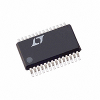
LTC1605-1CG#TRPBF Linear Technology, LTC1605-1CG#TRPBF Datasheet - Page 15

LTC1605-1CG#TRPBF
Manufacturer Part Number
LTC1605-1CG#TRPBF
Description
IC A/D CONV 16BIT SAMPLNG 28SSOP
Manufacturer
Linear Technology
Datasheet
1.LTC1605-1CGPBF.pdf
(20 pages)
Specifications of LTC1605-1CG#TRPBF
Number Of Bits
16
Sampling Rate (per Second)
100k
Data Interface
Parallel
Number Of Converters
1
Power Dissipation (max)
80mW
Voltage Supply Source
Analog and Digital
Operating Temperature
0°C ~ 70°C
Mounting Type
Surface Mount
Package / Case
28-SSOP (0.200", 5.30mm Width)
Lead Free Status / RoHS Status
Lead free / RoHS Compliant
Available stocks
Company
Part Number
Manufacturer
Quantity
Price
The circuit in Figure 16 is an example showing the LTC1605
16-bit A/D converter and LTC1391 8-channel MUX con-
nected to a 68HC11 controller. The LTC1605’s 16-bit data
output is read in two 8-bit bytes using Pins 6 (MSB, Bit7)
through 13 (Bit8, Bit0), connected to the HC11’s PORTC.
The MUX’s 4-bit serial address data is sent using the
controller’s SPI.
The process to convert a channel’s input signal is shown
in sample listing A. It begins with shifting in the MUX’s
channel data while the SS signal is a logic high. The MUX
channel address is latched on the falling edge of SS and the
Sample Listing A
*************************************************************************
*
* This example program selects the an LTC1391 MUX channel, initiates a *
* conversion, and retrieves conversion data. It stores the 16-bit data *
* in two consecutive memory locations. The program is designed for use *
* with the LTC1605’s /CS tied to ground (see timing diagram in
* Figure 17).
*
*************************************************************************
*
*****************************************
* 68HC11 register definitions
*****************************************
*
PORTA
*
*
*
PIOC
*
PORTC
*
DDRC
*
*
PORTD
*
DDRD
SPCR
*
SPSR
*
SPDR
*
* RAM variables to hold the LTC1605’s 14 conversion result
*
DIN1
DIN2
MUX
*
TYPICAL APPLICATIO S
EQU
EQU
EQU
EQU
EQU
EQU
EQU
EQU
EQU
EQU
EQU
EQU
$1000
$1002
$1003
$1007
$1008
$1009
$1028
$1029
$102A
$00
$01
$02
Parallel port A
Use Bit0 as an input for the LTC1605’s /BUSY signal
Use Bit3 as an output driving the LTC1605’s BYTE
input
Parallel I/O control register
“STAF,STAI,CWOM,HNDS, OIN, PLS, EGA,INVB”
Port C data register
“Bit7,Bit6,Bit5,Bit4,Bit3,Bit2,Bit1,Bit0”
Port D data direction register
“Bit7,Bit6,Bit5,Bit4,Bit3,Bit2,Bit1,Bit0”
1 = output, 0 = input
Port D data register
“ -
Port D data direction register
SPI control register
“SPIE,SPE ,DWOM,MSTR;SPOL,CPHA,SPR1,SPR0”
SPI status register
“SPIF,WCOL, -
SPI data register; Read-Buffer; Write-Shifter
This memory location holds the LTC1605’s bits 15 - 08
This memory location holds the LTC1605’s bits 07 - 00
This memory location holds the MUX address data
, -
U
, SS* ,CSK ;MOSI,MISO,TxD ,RxD “
,MODF; -
*
, -
, -
chosen channel’s input is applied at the LTC1605’s input,
Pin 1. Through the processor’s PORTA, a low-going pulse
is applied to the LTC1605’s R/C pin, initiating a conver-
sion. The processor then monitors the BUSY output.
When this signal becomes a logic high, signaling the end
of conversion, the processor reads the high byte of the
conversion through PORTC. The low byte is read through
PORTC when the processor changes the BYTE signal to a
logic high. The timing relationship of the control signals
and data are shown in Figure 17.
, -
“
*
*
*
LTC1605-1/LTC1605-2
*
15


