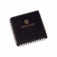
TC850CLW Microchip Technology, TC850CLW Datasheet - Page 8

TC850CLW
Manufacturer Part Number
TC850CLW
Description
IC ADC 15BIT FAST 44PLCC
Manufacturer
Microchip Technology
Datasheet
1.TC850CPL.pdf
(26 pages)
Specifications of TC850CLW
Data Interface
Parallel
Number Of Bits
15
Sampling Rate (per Second)
40
Number Of Converters
1
Voltage Supply Source
Dual ±
Operating Temperature
0°C ~ 70°C
Mounting Type
Surface Mount
Package / Case
44-PLCC
Resolution (bits)
15bit
Sampling Rate
40SPS
Input Channel Type
Differential
Supply Voltage Range - Analog
± 5V
Supply Current
2mA
Digital Ic Case Style
LCC
Lead Free Status / RoHS Status
Lead free / RoHS Compliant
Available stocks
Company
Part Number
Manufacturer
Quantity
Price
Company:
Part Number:
TC850CLW
Manufacturer:
MICROCHIP
Quantity:
12 000
Company:
Part Number:
TC850CLW
Manufacturer:
Microchip Technology
Quantity:
10 000
Part Number:
TC850CLW
Manufacturer:
TELCOM
Quantity:
20 000
Company:
Part Number:
TC850CLW713
Manufacturer:
MICROCHIP
Quantity:
12 000
Company:
Part Number:
TC850CLW713
Manufacturer:
Microchip Technology
Quantity:
10 000
TC850
3.0
The TC850 is a multiple-slope, integrating A/D con-
verter (ADC). The multiple-slope conversion process,
combined with chopper-stabilized amplifiers, results in
a significant increase in ADC speed, while maintaining
very high resolution and accuracy.
3.1
The conventional dual-slope converter measurement
cycle (shown in Figure 3-1) has two distinct phases:
1.
2.
FIGURE 3-1:
The input signal being converted is integrated for a
fixed time period, measured by counting clock pulses.
An opposite polarity constant reference voltage is then
de-integrated until the integrator output voltage returns
to zero. The reference integration time is directly
proportional to the input signal.
In a simple dual-slope converter, complete conversion
requires the integrator output to “ramp-up” and “ramp-
down.” Most dual-slope converters add a third phase,
auto-zero. During auto-zero, offset voltages of the input
buffer, integrator and comparator are nulled, thereby
eliminating the need for zero offset adjustments.
Dual-slope converter accuracy is unrelated to the inte-
grating resistor and capacitor values, as long as they
are stable during a measurement cycle. By converting
the unknown analog input voltage into an easily mea-
sured function of time, the dual-slope converter
reduces the need for expensive, precision passive
components.
Noise immunity is an inherent benefit of the integrating
conversion method. Noise spikes are integrated, or
averaged, to zero during the integration period. Inte-
grating ADCs are immune to the large conversion
errors
converters in high-noise environments.
A simple mathematical equation relates the input
signal, reference voltage and integration time:
DS21479C-page 8
Integrator
Output
Input signal integration
Reference voltage integration (de-integration).
DETAILED DESCRIPTION
Dual-Slope Conversion Principles
that
Auto
Zero
plague
Time
Dual-Slope ADC Cycle
successive
Signal De-integrate
Reference
De-integrate
End of Conversion
approximation
0V
EQUATION 3-1:
3.2
One limitation of the dual-slope measurement tech-
nique is conversion speed. In a typical dual-slope
method, the auto-zero and integrate times are each
one-half of the de-integrate time. For a 15-bit conver-
sion, 2
for auto-zero, integrate and de-integrate phases,
respectively. The large number of clock cycles
effectively limits the conversion rate to about 2.5
conversions per second, when a typical analog CMOS
fabrication process is used.
The TC850 uses a multiple-slope conversion technique
to increase conversion speed (Figure 3-2). This tech-
nique makes use of a two-slope de-integration phase
and permits 15-bit resolution up to 40 conversions per
second.
During the TC850’s de-integration phase, the integra-
tion capacitor is rapidly discharged to yield a
resolution of 9 bits. At this point, some charge will
remain on the capacitor. This remaining charge is then
slowly de-integrated, producing an additional 6 bits of
resolution. The result is 15 bits of resolution achieved
with only 2
de-integration. A complete conversion cycle occupies
only 1280 clock pulses.
In order to generate “fast-slow” de-integration phases,
two voltage references are required. The primary refer-
ence (V
(typically V
secondary voltage reference (V
(typically 25.6 mV). To maintain 15-bit linearity, a
tolerance of 0.5% for V
FIGURE 3-2:
Integration Cycle
where:
Integrator
Output
Signal Integrate
14
R
T
T
REF1
V
INT
INT
DEINT
Multiple-Slope Conversion
Principles
+ 2
REF
REF1
9
1
Auto
Zero
C
14
) is set to one-half of the full scale voltage
+ 2
INT
+ 2
= Reference voltage
= Signal integration time (fixed)
= Reference voltage integration time
6
Time
∫
= 1.6384V, and V
(variable).
T
0
15
(512 + 64, or 576) clock pulses for
INT
(65,536) clock pulses are required
V
“Fast Slow” Reference De-
REF2
© 2006 Microchip Technology Inc.
IN
(T)DT =
"Fast" Reference
De-integrate
(9-Bit Resolution)
is recommended.
REF2
"Slow" Reference De-integrate
(6-Bit Resolution)
V
FS
) is set to V
REF
R
End of Conversion
INT
= 3.2768V). The
T
C
DEINT
INT
0V
REF1
/64


