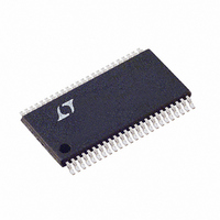
LTC1744IFW#TR Linear Technology, LTC1744IFW#TR Datasheet - Page 12

LTC1744IFW#TR
Manufacturer Part Number
LTC1744IFW#TR
Description
IC ADC 14BIT 50MSPS 48-TSSOP
Manufacturer
Linear Technology
Datasheet
1.LTC1744CFWPBF.pdf
(24 pages)
Specifications of LTC1744IFW#TR
Number Of Bits
14
Sampling Rate (per Second)
50M
Data Interface
Parallel
Number Of Converters
1
Power Dissipation (max)
1.5W
Voltage Supply Source
Single Supply
Operating Temperature
-40°C ~ 85°C
Mounting Type
Surface Mount
Package / Case
48-TFSOP (0.240", 6.10mm Width)
Lead Free Status / RoHS Status
Contains lead / RoHS non-compliant
Other names
LTC1744IFWTR
Available stocks
Company
Part Number
Manufacturer
Quantity
Price
LTC1744
APPLICATIO S I FOR ATIO
The LTC1744 has two phases of operation, determined by
the state of the differential ENC/ENC input pins. For brev-
ity, the text will refer to ENC greater than ENC as ENC high
and ENC less than ENC as ENC low.
Each pipelined stage shown in Figure 1 contains an ADC,
a reconstruction DAC and an interstage residue amplifier.
In operation, the ADC quantizes the input to the stage and
the quantized value is subtracted from the input by the
DAC to produce a residue. The residue is amplified and
output by the residue amplifier. Successive stages operate
out of phase so that when the odd stages are outputting
their residue, the even stages are acquiring that residue
and visa versa.
When ENC is low, the analog input is sampled differentially
directly onto the input sample-and-hold capacitors, inside
the “Input S/H” shown in the block diagram. At the instant
that ENC transitions from low to high, the sampled input
is held. While ENC is high, the held input voltage is
buffered by the S/H amplifier which drives the first pipelined
ADC stage. The first stage acquires the output of the S/H
during this high phase of ENC. When ENC goes back low,
12
SENSE
4.7 F
A
A
V
IN
IN
CM
+
–
INPUT
REFERENCE
S/H
SELECT
RANGE
2.5V
U
REF
BUF
U
FIRST STAGE
ADC STAGE
PIPELINED
5-BIT
W
AMP
DIFF
REF
REFLB
0.1 F
1 F
REFL
REFHA
U
4.7 F
Figure 1. Block Diagram
SECOND STAGE
REFH
ADC STAGE
PIPELINED
REFLA REFHB
0.1 F
4-BIT
1 F
INTERNAL CLOCK SIGNALS
DIFFERENTIAL
the first stage produces its residue which is acquired by
the second stage. At the same time, the input S/H goes
back to acquiring the analog input. When ENC goes back
high, the second stage produces its residue which is
acquired by the third stage. An identical process is re-
peated for the third stage, resulting in a third stage residue
that is sent to the fourth stage ADC for final evaluation.
Each ADC stage following the first has additional range to
accommodate flash and amplifier offset errors. Results
from all of the ADC stages are digitally delayed such that
the results can be properly combined in the correction
logic before being sent to the output buffer.
SAMPLE/HOLD OPERATION AND INPUT DRIVE
Sample Hold Operation
Figure 2 shows an equivalent circuit for the LTC1744
CMOS differential sample-and-hold. The differential ana-
log inputs are sampled directly onto sampling capacitors
(C
capacitor sampling results in lowest possible noise for a
LOW JITTER
DRIVER
CLOCK
INPUT
ENC
SAMPLE
ENC
) through CMOS transmission gates. This direct
THIRD STAGE
ADC STAGE
PIPELINED
CALIBRATION LOGIC
CONTROL LOGIC
4-BIT
MSBINV
AND
OE
AND CORRECTION
SHIFT REGISTER
FOURTH STAGE
DRIVERS
OUTPUT
FLASH
4-BIT
ADC
OGND
1744 F01
OV
OF
D13
D0
CLKOUT
•
•
•
DD
0.5V TO
5V
1744f


