CS5345-CQZR Cirrus Logic Inc, CS5345-CQZR Datasheet
CS5345-CQZR
Specifications of CS5345-CQZR
Available stocks


Related parts for CS5345-CQZR


CS5345-CQZR Summary of contents
Page 1
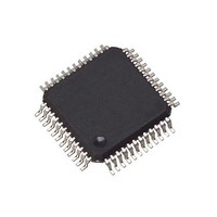
... Integrated level translators allow easy interfacing be- tween the CS5345 and other devices operating over a wide range of logic levels. The CS5345 is available in a 48-pin LQFP package in Commercial (-10° to +70° C) and Automotive (-40° to +105° C) grade. The CDB5345 Customer Demonstra- tion board is also available for device evaluation and implementation suggestions. Please refer to Information” ...
Page 2
... High-Pass Filter Freeze (Bit 1) .............................................................................................. 32 6.3.5 Master / Slave Mode (Bit 0) ................................................................................................... 32 6.4 MCLK Frequency - Address 05h .................................................................................................... 33 6.4.1 Master Clock Dividers (Bits 6:4) ............................................................................................ 33 6.5 PGAOut Control - Address 06h ...................................................................................................... 33 6.5.1 PGAOut Source Select (Bit 6) ............................................................................................... 33 6.6 Channel B PGA Control - Address 07h .......................................................................................... 33 2 ......................................................................................................................... 5 CS5345 DS658F2 ...
Page 3
... Figure 20.Double-Speed Passband Ripple ............................................................................................... 39 Figure 21.Quad-Speed Stopband Rejection ............................................................................................. 39 Figure 22.Quad-Speed Stopband Rejection ............................................................................................. 39 Figure 23.Quad-Speed Transition Band (Detail) ....................................................................................... 39 Figure 24.Quad-Speed Passband Ripple ................................................................................................. 39 LIST OF TABLES Table 1. Speed Modes .............................................................................................................................. 23 Table 2. Common Clock Frequencies ....................................................................................................... 23 Table 3. Slave Mode Serial Bit Clock Ratios ............................................................................................. 24 Table 4. Device Revision .......................................................................................................................... 31 DS658F2 ........................................................................................................ 41 CS5345 3 ...
Page 4
... Table 5. Freeze-able Bits .......................................................................................................................... 31 Table 6. Functional Mode Selection .......................................................................................................... 32 Table 7. Digital Interface Formats ............................................................................................................. 32 Table 8. MCLK Frequency ........................................................................................................................ 33 Table 9. PGAOut Source Selection ........................................................................................................... 33 Table 10. Example Gain and Attenuation Settings ................................................................................... 34 Table 11. PGA Soft Cross or Zero Cross Mode Selection ........................................................................ 35 Table 12. Analog Input Multiplexer Selection ............................................................................................ 35 4 CS5345 DS658F2 ...
Page 5
... Stereo Analog Input 3 (Input) - The full-scale level is specified in the ADC Analog Characteristics AIN3B 8 specification table. AIN2A 9 Stereo Analog Input 2 (Input) - The full-scale level is specified in the ADC Analog Characteristics AIN2B 10 specification table. DS658F2 CS5345 Mode. CS5345 VLS 36 35 TSTO AGND 31 AGND PGAOUTB ...
Page 6
... Master Clock (Input) - Clock source for the ADC’s delta-sigma modulators. DGND 45 Digital Ground (Input) - Ground reference for the internal digital section Digital Power (Input) - Positive power for the internal digital section. INT 47 Interrupt (Output) - Indicates an interrupt condition has occurred. OVFL 48 Overflow (Output) - Indicates an ADC overflow condition is present. 6 33. CS5345 DS658F2 ...
Page 7
... Analog VA Digital VD Logic - Serial Port VLS Logic - Control Port VLC (Note AGND-0.3 INA V Logic - Serial Port IND-S Logic - Control Port V IND stg CS5345 Nom Max Units 5.0 5.25 V 3.3 (Note 1) V 3.3 5.25 V 3.3 5.25 V °C - +70 - +105 °C Min Max Units -0 ...
Page 8
... A Figure 7 on page 22. Line-Level Inputs Commercial Grade Symbol Min Typ 98 104 95 101 - (Note -95 - - -92 THD -92 - -75 - - 101 (Note -92 - - THD -89 - - -81 CS5345 = -10° to +70° C for Commercial or -40° to Automotive Grade Max Min Typ Max - 96 104 - - 93 101 - - - -89 - - -92 - -86 - - 101 - - ...
Page 9
... Symbol Min Typ - ± - 100 0.51*VA 0.57*VA 0.63*VA 0.51*VA 0.57*VA 0.63*VA (Note 4) 6.12 6 Line-Level and Microphone-Level Inputs Commercial Grade Symbol Min Typ - 0 CS5345 Automotive Grade Max Min Typ Max Unit - - 90 - ± 10 ± ± 100 - ppm/°C 7.48 5.44 6.8 8.16 ...
Page 10
... Valid for Double- and Quad-Speed Modes only. 7. Valid when the microphone-level inputs are selected. 10 Microphone-Level Inputs Commercial Grade Symbol Min Typ (Note -80 - -60 THD (Note -80 - -60 THD ± ± - 300 0.013*VA 0.017*VA 0.021*VA 0.013*VA 0.017*VA 0.021*VA (Note CS5345 Automotive Grade Max Min Typ Max - -74 - - -74 - - ...
Page 11
... Response is clock-dependent and will scale with Fs. Note that the response plots normalized to Fs and can be de-normalized by multiplying the X-axis scale by Fs. DS658F2 Symbol Min Typ 0.5688 - 12/ 0.5604 - 9/ 0.5000 - 5/ (Note 9) 20 (Note /Fs (Figures 13 CS5345 Max Unit 0.4896 Fs 0.035 0.4896 Fs 0.025 0.2604 Fs 0.025 Deg 24) are 11 ...
Page 12
... Referred to the typical Line-Level Full-Scale Input Voltage -10° to +70° C for Commercial or -40° 4. 5.25 V Commercial Grade Symbol Min Typ 98 104 95 101 (Note 11 -80 - -81 - -41 THD -80 - - (Note 11 -74 - -60 THD -68 CS5345 Figure 7 on page 22. Automotive Grade Max Min Typ Max - 96 104 - - 93 101 - - -74 - - -41 - -74 - - ...
Page 13
... PGA Setting: +12 dB A-weighted unweighted Total Harmonic Distortion + Noise PGA Setting: - PGA Setting: +12 dB DS658F2 3.46 V Commercial Grade Symbol Min Typ 93 101 (Note 11 -80 - -78 - -38 THD -80 - - (Note 11 -74 - -60 THD -68 CS5345 Automotive Grade Max Min Typ Max - 91 101 - - -74 - - -38 - -74 - - ...
Page 14
... 5.25 V Commercial Grade Symbol Min Typ - 0.1 ± ± - 100 - 0.3 ± ± - 300 (Note 12) -0.1dB - - 180 OUT R 100 - CS5345 Automotive Grade Max Min Typ Max Unit - - 0.1 - ± ± 100 - ppm/° 0.3 - ± ± 300 - ppm/°C +0.1dB -0.1dB - +0 ...
Page 15
... Guaranteed by design. The DC current draw represents the allowed current draw due to typical leakage through the electrolytic de-coupling capacitors. DS658F2 Symbol 3 VD, VLS, VLC = VD, VLS, VLC = 3 VLS, VLC, VD (Note 14) PSRR VQ (Note 15 FILT+ MICBIAS I MB CS5345 Min Typ Max - 0. 0. 400 485 - 198 241 - 4 0 ...
Page 16
... Symbol Min Serial Port V 0.8xVLS IH Control Port V 0.8xVLC IH Serial Port V 0.7xVLS IH Control Port V 0.7xVLC IH Serial Port Control Port Serial Port V VLS-1.0 OH Control Port V VLC-1.0 OH Serial Port Control Port (Note 17 ---------------- - LRCK CS5345 Typ Max Units - - 0.2xVLS V - 0.2xVLC 0 0.4 V μA - ± μ DS658F2 ...
Page 17
... Symbol Single-Speed Mode Fs Double-Speed Mode Fs Quad-Speed Mode Fs f 1.024 mclk t clkhl t slr t sdo Single-Speed Mode t -------------------- - sclkw ( 128 Double-Speed Mode t ----------------- - sclkw ( 64 Quad-Speed Mode t ----------------- - sclkw ( 64 t sclkh t sclkl t slr t sdo 18. CS5345 Min Typ Max Unit kHz 50 - 100 kHz 100 - 200 kHz - 51.200 MHz - )Fs ...
Page 18
... LRCK Output SCLK Output SDOUT Figure 1. Master Mode Serial Audio Port Timing LRCK Input SCLK Input SDOUT 18 t slr t sdo t t sclkh slr t sclkw t sdo Figure 2. Slave Mode Serial Audio Port Timing CS5345 t sclkl DS658F2 ...
Page 19
... Channel A - Left LRCK SCLK SDATA MSB - Figure 3. Format 0, Left-Justified up to 24-Bit Data Channel A - Left LRCK SCLK SDATA +5 +4 MSB - DS658F2 + LSB MSB - LSB MSB -1 Figure 4. Format 1, I² 24-Bit Data CS5345 Channel B - Right - LSB Channel B - Right + LSB 19 ...
Page 20
... Figure 5. Control Port Timing - I²C Format CS5345 Min Max - 100 500 - 4.7 - 4.0 - 4.7 - 4 250 - - 300 fd 4.7 - 300 1000 , of SCL ate d Sta rt ...
Page 21
... CS t css CCLK CDIN CDOUT DS658F2 = 30 pF. L Symbol f sck t srs t csh t css t scl t sch t dsu (Note 21 (Note 22 (Note 22 srs t scl t sch dsu Figure 6. Control Port Timing - SPI Format CS5345 Min Max Units - 6.0 MHz 500 - ns 1.0 - μ 100 ns - 100 ns t csh 21 ...
Page 22
... TSTO 1800 pF AIN6B MICBIAS VQ AGND FILT+ AGND AFILTA AFILTB AGND * Capacitors must be C0G or equivalent DGND Figure 7. Typical Connection Diagram CS5345 +3.3V to +5V 10 µF 3.3 µF 3.3 µF Left Analog Input 1 100 Ω µF 100 kΩ µF 100 kΩ 100 Ω Right Analog Input 1 Left Analog Input 2 100 Ω ...
Page 23
... The desired register settings can be loaded while the PDN bit remains set. 4. Clear the PDN bit to initiate the power-up sequence. 4.2 System Clocking The CS5345 will operate at sampling frequencies from 4 kHz to 200 kHz. This range is divided into three speed modes as shown in 4.2.1 Master Clock MCLK/LRCK must maintain an integer ratio as shown in frequency at which audio samples for each channel are clocked out of the device ...
Page 24
... High-Pass Filter and DC Offset Calibration When using operational amplifiers in the input circuitry driving the CS5345, a small DC offset may be driven into the A/D converter. The CS5345 includes a high-pass filter after the decimator to remove any DC offset which could result in recording a DC level, possibly yielding clicks when switching between devices in a mul- tichannel system ...
Page 25
... PGA Auxiliary Analog Output The CS5345 includes an auxiliary analog output through the PGAOUT pins. These pins can be configured to output the analog input to the ADC as selected by the input MUX and gained or attenuated with the PGA, or alternatively, they may be set to high-impedance. See the for information on configuring the PGA auxiliary analog output ...
Page 26
... The control port has two modes: SPI and I²C, with the CS5345 acting as a slave device. SPI Mode is se- lected if there is a high-to-low transition on the AD0/CS pin, after the RESET pin has been brought high. I²C Mode is selected by connecting the AD0/CS pin through a resistor to VLC or DGND, thereby permanently selecting the desired AD0 bit address state ...
Page 27
... SDA while the clock is high. A Stop condition is a rising transition while the clock is high. All other transitions of SDA occur while the clock is low. The first byte sent to the CS5345 after a Start condition consists of a 7-bit chip address field and a R/W bit (high for a read, low for a write). ...
Page 28
... CS5345s in the system. If only one master clock source is needed, one solution is to place one CS5345 in Master Mode, and slave all of the other CS5345s to the one master. If multiple master clock sources are needed, a possible solution would be to supply all clocks from the same external source and time the CS5345 reset with the inactive edge of master clock ...
Page 29
... VD. Power supply decoupling capacitors should be as near to the CS5345 as possible, with the low value ceramic capacitor being the nearest. All signals, espe- cially clocks, should be kept away from the FILT+ and VQ pins in order to avoid unwanted coupling into the modulators. The FILT+ and VQ decoupling capacitors, particularly the 0.1 µ ...
Page 30
... Freq1 Freq0 Reserved Reserved Reserved Gain5 Gain4 Gain3 Gain5 Gain4 Gain3 PGASoft PGAZero Reserved Reserved ClkErr ClkErrM ClkErr1 ClkErr0 CS5345 REV2 REV1 PDN_ADC Reserved Reserved Reserved Reserved Mute HPFFreeze Reserved Reserved Reserved Reserved Reserved Reserved Gain2 Gain1 Gain2 Gain1 Sel2 Sel1 1 0 ...
Page 31
... DS658F2 PART0 REV3 Table 4 REV[2:0] Revision 001 010 B, C0 011 Table 4. Device Revision Reserved PDN_MIC Name Register Mute 04h 07h 08h Table 5. Freeze-able Bits CS5345 2 1 REV2 REV1 below PDN_ADC Reserved Bit(s) 2 5:0 5:0 0 REV0 0 PDN 31 ...
Page 32
... Double-Speed Mode 100 kHz sample rates Quad-Speed Mode: 100 to 200 kHz sample rates Reserved Table 6. Functional Mode Selection Table 7 and may be seen in Description I² 24-bit data Table 7. Digital Interface Formats “High-Pass Filter and DC Offset Calibration” on CS5345 2 1 Mute HPFFreeze Figure 3 and Figure 4. Format ...
Page 33
... MCLK Freq2 MCLK Freq1 Table 8. MCLK Frequency Reserved Reserved PGAOut PGAOutA & PGAOutB 0 High Impedance 1 PGA Output Table 9. PGAOut Source Selection Gain4 Gain3 CS5345 2 1 Reserved Reserved Reserved for the appropriate settings. MCLK Freq0 Reserved Reserved Reserved 2 1 Gain2 Gain1 Gain0 ...
Page 34
... The zero cross function is independently mon- itored and implemented for each channel. See Gain4 Gain3 Gain[5:0] Setting 101000 -12 dB 000000 0 dB 011000 + PGASoft PGAZero 11. Table 11. CS5345 Gain2 Gain1 Gain0 Table 10 for ex Sel2 Sel1 Sel0 DS658F2 ...
Page 35
... Microphone-Level Inputs (+32 dB Gain Enabled Table 12. Analog Input Multiplexer Selection Reserved Reserved Reserved ClkErr CS5345 Mode Table 12. PGA/ADC Input Line-Level Input Pair 1 Line-Level Input Pair 2 Line-Level Input Pair 3 Line-Level Input Pair 4 Line-Level Input Pair 5 Line-Level Input Pair 6 Reserved 2 1 Reserved Reserved Active_H ...
Page 36
... INT pin becomes active on the removal of the interrupt condition. In Level-Active Mode, the INT pin re- mains active during the interrupt condition Rising edge active 01 - Falling edge active 10 - Level active 11 - Reserved Reserved ClkErrM Reserved ClkErr1 Reserved ClkErr0 CS5345 Reserved OvflM UndrflM “Interrupt Status - Ad Reserved Ovfl1 Undrfl1 Reserved Ovfl0 Undrfl0 DS658F2 ...
Page 37
... Units in deci- bels. Interchannel Gain Mismatch The gain difference between left and right channels. Units in decibels. Gain Drift The change in gain value with temperature. Units in ppm/°C. DS658F2 CS5345 37 ...
Page 38
... Figure 18. Double-Speed Stopband Rejection CS5345 0.46 0.48 0.50 0.52 0.54 0.56 0.58 Frequency (norm alized to Fs) 0.05 0.1 0.15 0.2 0.25 0.3 0.35 0.4 0.45 Frequency (norm alized to Fs) ...
Page 39
... Figure 24. Quad-Speed Passband Ripple CS5345 0.10 0.15 0.20 0.25 0.30 0.35 0.40 0.45 0.50 Frequency (norm alized to Fs) Frequency (norm alized to Fs) Frequency (norm alized to Fs) ...
Page 40
... Symbol θ JA 48-LQFP θ JC CS5345 A A1 MILLIMETERS MIN NOM MAX --- 1.40 1.60 0.05 0.10 0.15 0.17 0.22 0.27 8.70 9.0 BSC 9.30 6.90 7.0 BSC 7 ...
Page 41
... CS5345 Container Order # Tray CS5345-CQZ Tape & Reel CS5345-CQZR Tray CS5345-DQZ Tape & Reel CS5345-DQZR - - CDB5345 Control Port Description and Timing description on page 31. 5. page 17. table on page 21. Channel A PGA Control - Address 08h ...