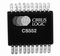
CS5523-ASZR Cirrus Logic Inc, CS5523-ASZR Datasheet - Page 33

CS5523-ASZR
Manufacturer Part Number
CS5523-ASZR
Description
IC ADC 16BIT 4CH 24-SSOP
Manufacturer
Cirrus Logic Inc
Datasheet
1.CS5521-ASZ.pdf
(56 pages)
Specifications of CS5523-ASZR
Number Of Bits
16
Data Interface
Serial
Number Of Converters
1
Power Dissipation (max)
10mW
Voltage Supply Source
Analog and Digital
Operating Temperature
-40°C ~ 85°C
Mounting Type
Surface Mount
Package / Case
24-SSOP
Lead Free Status / RoHS Status
Lead free / RoHS Compliant
perform a system gain calibration. In either case,
the calibration signals must be within the specified
calibration limits for each specific calibration step
(refer to the ‘System Calibration Specifications’ in
ANALOG CHARACTERISTICS). If a system gain
calibration is performed the following conditions
must be met:
1) Full-scale input must not saturate the 20X in-
DS317F8
Full Scale + -
Full Scale + -
Figure 15. System Calibration of Offset (High Ranges)
Figure 17. System Calibration of Gain (High Ranges)
Figure 16. System Calibration of Gain (Low Ranges)
CM + -
0V
strumentation amplifier, if the calibration is on
an input range where the instrumentation am-
plifier is involved.
CM + -
CM + -
External
Connections
+
-
External
Connections
External
Connections
AIN-
AIN+
AIN+
AIN-
AIN+
AIN-
+
-
+
-
X20
+
-
X20
X20
+
-
+
-
+
-
2) The 1’s density of the modulator must not be
3) The input must not be so small, relative to the
The converter’s input ranges were chosen to guar-
antee gain calibration accuracy to 1 LSB
LSB
This is useful when a user wants to manually scale
the full-scale range of the converter and maintain
accuracy. For example, if a gain calibration is per-
formed with a 2.5 V full-scale voltage and a 1.25 V
input range is desired, the user can read the con-
tents of the gain register, shift the register contents
left by 1 bit, and then write the result back to the
gain register. This multiplies the gain by 2.
Assuming a system can provide two known voltag-
es, the following equations allow the user to manu-
ally compute the calibration register’s values based
on two uncalibrated conversions (see note). The
offset and gain calibration registers are used to ad-
just a typical conversion as follows:
Calibration can be performed using the following
equations:
Note: Uncalibrated conversions imply that the gain and off-
greater than 80 percent (the input to the ΔΣ
modulator must not exceed the maximum input
which Table 1 specifies).
range chosen, that the resulting gain register’s
content,
3.9999998 (see the discussion of operating lim-
its on input span under the Analog Input and
Limitations in Calibration Range sections).
This requires the full-scale input voltage to the
modulator to be at least 25 percent of the nom-
inal value.
24
set registers are at default {gain register = 0x400000
(Hex) and offset register = 0x000000 (Hex)}.
when system gain calibration is performed.
where G = (Rc1 - Rc0)/(Ru1-Ru0).
Rc = (Ru + Co) * Cg / 2
decoded
Co = (Rc0/G - Ru0)
Cg = 2
CS5521/22/23/24/28
22
in
* G
decimal,
22
.
16
exceeds
or 16
33


