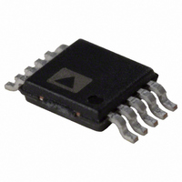
AD7787BRM Analog Devices Inc, AD7787BRM Datasheet

AD7787BRM
Specifications of AD7787BRM
Available stocks
Related parts for AD7787BRM
AD7787BRM Summary of contents
Page 1
FEATURES Power Supply: 2 5.25 V operation Normal mode: 75 µA max Power-down mode: 1 µA max RMS noise: 1.1 µV at 9.5 Hz update rate 19.5-bit p-p resolution (22 bits effective resolution) Integral nonlinearity: 3.5 ppm typical ...
Page 2
AD7787 TABLE OF CONTENTS Specifications..................................................................................... 3 Timing Characteristics..................................................................... 5 Absolute Maximum Ratings............................................................ 7 ESD Caution.................................................................................. 7 Pin Configuration and Function Descriptions............................. 8 Typical Performance Characteristics ............................................. 9 On-Chip Registers .......................................................................... 10 Communications Register (RS1, RS0 = 0, 0)........................... 10 Status ...
Page 3
SPECIFICATIONS Temperature range is −40°C to +105° unless otherwise noted. MAX Table 1. Parameter ADC CHANNEL SPECIFICATION Output Update Rate ADC CHANNEL 1 No Missing Codes Resolution Output Noise Integral Nonlinearity Offset Error Offset Error Drift vs. ...
Page 4
AD7787 Parameter LOGIC INPUTS 1 All Inputs Except SCLK V , Input Low Voltage INL V , Input High Voltage INH SCLK Only (Schmitt-Triggered Input) V (+) T V (− (+) − V (− (+) ...
Page 5
TIMING CHARACTERISTICS Sample tested during initial release to ensure compliance. All input signals are specified with t from a voltage level of 1.6 V (see Figure 3 and Figure 4 2 5.25 V; GND = 0 ...
Page 6
AD7787 DOUT/RDY (O) SCLK (I) I (1.6mA WITH V SINK 100µA WITH OUTPUT 1.6V PIN 50pF I (200µA WITH V SOURCE 100µA WITH V DD Figure 2. Load Circuit for Timing Characterization CS ( MSB ...
Page 7
ABSOLUTE MAXIMUM RATINGS T = 25°C, unless otherwise noted. A Table 3. Parameter V to GND DD Analog Input Voltage to GND Reference Input Voltage to GND Total AIN/REFIN Current (Indefinite) Digital Input Voltage to GND Digital Output Voltage to ...
Page 8
AD7787 PIN CONFIGURATION AND FUNCTION DESCRIPTIONS Table 4. Pin Function Descriptions Pin No. Mnemonic Function 1 SCLK Serial Clock Input for Data Transfers to and from the ADC. The SCLK has a Schmitt-triggered input, making the interface suitable for opto-isolated ...
Page 9
TYPICAL PERFORMANCE CHARACTERISTICS 0 –10 –20 –30 –40 –50 –60 –70 –80 –90 –100 –110 –120 100 FREQUENCY (Hz) Figure 6. Frequency Response with 16.6 Hz Update Rate 100 V = ...
Page 10
AD7787 ON-CHIP REGISTERS The ADC is controlled and configured via a number of on-chip registers, which are described on the following pages. In the following descriptions, set implies a Logic 1 state and cleared implies a Logic 0 state, unless ...
Page 11
Table 7. Channel Selection CH1 CH0 STATUS REGISTER (RS1, RS0 = 0, 0; POWER-ON/RESET = 0×8C) The status register is an 8-bit read-only register. To access the ADC status register, the user ...
Page 12
AD7787 MODE REGISTER (RS1, RS0 = 0, 1; POWER-ON/RESET = 0×02) The mode register is an 8-bit register from which data can be read or to which data can be written. This register is used to configure the ADC for ...
Page 13
FILTER REGISTER (RS1, RS0 = 1, 0; POWER-ON/RESET = 0×04) The filter register is an 8-bit register from which data can be read or to which data can be written. This register is used to set the output word rate. ...
Page 14
AD7787 ADC CIRCUIT INFORMATION OVERVIEW The AD7787 is a low power ADC that incorporates an Σ-Δ modulator, a buffer, and an on-chip digital filter intended for the measurement of wide dynamic range, low frequency signals, such as those in pressure ...
Page 15
DIGITAL INTERFACE As previously outlined, the AD7787’s programmable functions are controlled using a set of on-chip registers. Data is written to these registers via the part’s serial interface and read access to the on-chip registers is also provided by this ...
Page 16
AD7787 Single Conversion Mode In single conversion mode, the AD7787 is placed in shutdown mode between conversions. When a single conversion is initiated by setting MD1 to 1 and MD0 the mode register, the AD7787 powers up, ...
Page 17
Continuous Read Mode Rather than write to the communications register each time a conversion is complete to access the data, the AD7787 can be placed in continuous read mode. By writing 00111100 (Channel AIN1) or 00111101 (Channel AIN2) to the ...
Page 18
AD7787 CIRCUIT DESCRIPTION ANALOG INPUT CHANNEL The AD7787 has two analog input channels that are connected to the on-chip buffer amplifier when the device is operated in buffered mode and directly to the modulator when the device is operated in ...
Page 19
Reference voltage sources like those previously recommended, e.g., ADR391, will typically have low output impedances and are, therefore, tolerant to having decoupling capacitors on REFIN without introducing gain errors in the system. Deriving the reference input voltage across an external ...
Page 20
... AD7787 OUTLINE DIMENSIONS ORDERING GUIDE Models Temperature Range AD7787BRM −40°C to +105°C AD7787BRM-REEL −40°C to +105°C EVAL-AD7787EB © 2004 Analog Devices, Inc. All rights reserved. Trademarks and registered trademarks are the property of their respective owners. 3.00 BSC 10 6 4.90 BSC 3 ...


