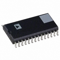
AD9220AR Analog Devices Inc, AD9220AR Datasheet - Page 9

AD9220AR
Manufacturer Part Number
AD9220AR
Description
IC ADC 12BIT 10MSPS 28-SOIC
Manufacturer
Analog Devices Inc
Datasheet
1.AD9220ARSZ-REEL.pdf
(32 pages)
Specifications of AD9220AR
Mounting Type
Surface Mount
Rohs Status
RoHS non-compliant
Number Of Bits
12
Sampling Rate (per Second)
10M
Data Interface
Parallel
Number Of Converters
7
Power Dissipation (max)
310mW
Voltage Supply Source
Single Supply
Operating Temperature
-40°C ~ 85°C
Package / Case
28-SOIC (0.300", 7.50mm Width)
Power Dissipation Pd
310mW
Input Channels Per Adc
1
No. Of Channels
1
Peak Reflow Compatible (260 C)
No
Sample Rate
10MSPS
Supply Voltage Max
5V
No. Of Bits
12 Bit
For Use With
AD9220-EB - BOARD EVAL FOR AD9220
Lead Free Status / RoHS Status
Contains lead / RoHS non-compliant
Available stocks
Company
Part Number
Manufacturer
Quantity
Price
Part Number:
AD9220AR
Manufacturer:
ADI/亚德诺
Quantity:
20 000
Company:
Part Number:
AD9220ARS
Manufacturer:
AD
Quantity:
5 510
Part Number:
AD9220ARS
Manufacturer:
ADI/亚德诺
Quantity:
20 000
Part Number:
AD9220ARSZ
Manufacturer:
ADI/亚德诺
Quantity:
20 000
Part Number:
AD9220ARSZ-REEL
Manufacturer:
ADI/亚德诺
Quantity:
20 000
Part Number:
AD9220ARSZRL
Manufacturer:
ADI/亚德诺
Quantity:
20 000
INTRODUCTION
The AD9221/AD9223/AD9220 are members of a high perfor-
mance, complete single-supply 12-bit ADC product family based
on the same CMOS pipelined architecture. The product family
allows the system designer an upward or downward component
selection path based on dynamic performance, sample rate, and
power. The analog input range of the AD9221/AD9223/AD9220
is highly flexible, allowing for both single-ended or differen-
tial inputs of varying amplitudes that can be ac or dc coupled.
Each device shares the same interface options, pinout, and
package offering.
The AD9221/AD9223/AD9220 utilize a four-stage pipeline
architecture with a wideband input sample-and-hold amplifier
(SHA) implemented on a cost-effective CMOS process. Each
stage of the pipeline, excluding the last stage, consists of a low
resolution flash A/D connected to a switched capacitor DAC
and interstage residue amplifier (MDAC). The residue amplifier
amplifies the difference between the reconstructed DAC output
and the flash input for the next stage in the pipeline. One bit of
redundancy is used in each of the stages to facilitate digital
correction of flash errors. The last stage simply consists of a
flash A/D.
The pipeline architecture allows a greater throughput rate at the
expense of pipeline delay or latency. This means that while the
converter is capable of capturing a new input sample every clock
cycle, it actually takes three clock cycles for the conversion to be
fully processed and appear at the output. This latency is not a
concern in most applications. The digital output, together with
the out-of-range indicator (OTR), is latched into an output buffer
to drive the output pins. The output drivers can be configured to
interface with 5 V or 3.3 V logic families.
The AD9221/AD9223/AD9220 use both edges of the clock in
their internal timing circuitry (see Figure 1 and Specifications
for exact timing requirements). The A/D samples the analog
input on the rising edge of the clock input. During the clock low
time (between the falling edge and rising edge of the clock), the
input SHA is in the sample mode; during the clock high time, it
is in hold. System disturbances just prior to the rising edge of
the clock and/or excessive clock jitter may cause the input SHA
to acquire the wrong value, and should be minimized.
The internal circuitry of both the input SHA and individual
pipeline stages of each member of the product family are opti-
mized for both power dissipation and performance. An inherent
trade-off exists between the input SHA’s dynamic performance
and its power dissipation. Figures 2 and 3 show this trade-off by
comparing the full-power bandwidth and settling time of the
AD9221/AD9223/AD9220. Both figures reveal that higher full-
power bandwidths and faster settling times are achieved at the
expense of an increase in power dissipation. Similarly, a trade-
off exists between the sampling rate and the power dissipated
in each stage.
As previously stated, the AD9221, AD9223, and AD9220 are
similar in most aspects except for the specified sampling rate,
power consumption, and dynamic performance. The product
family is highly flexible, providing several different input ranges
and interface options. As a result, many of the application issues
and trade-offs associated with these resulting configurations are
REV. E
–9–
also similar. The data sheet is structured such that the designer
can make an informed decision in selecting the proper A/D and
optimizing its performance to fit the specific application.
ANALOG INPUT AND REFERENCE OVERVIEW
Figure 4, a simplified model of the AD9221/AD9223/AD9220,
highlights the relationship between the analog inputs, VINA,
VINB, and the reference voltage, VREF. Like the voltage
applied to the top of the resistor ladder in a flash A/D converter,
the value VREF defines the maximum input voltage to the A/D
core. The minimum input voltage to the A/D core is automati-
cally defined to be –VREF.
Figure 4. AD9221/AD9223/AD9220 Equivalent
Functional Input Circuit
4000
3000
2000
1000
–12
–3
–6
–9
0
0
1
0
AD9220
Figure 2. Full-Power Bandwidth
VINA
VINB
Figure 3. Settling Time
AD9221/AD9223/AD9220
10
AD9221/AD9223/AD9220
V
CORE
20
SETTLING TIME – ns
FREQUENCY – MHz
AD9223
10
30
+V
CORE
–V
AD9223
A/D
REF
REF
AD9221
40
AD9221
12
AD9220
50
100
60


