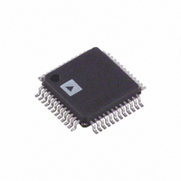
AD7661ASTZ Analog Devices Inc, AD7661ASTZ Datasheet - Page 5

AD7661ASTZ
Manufacturer Part Number
AD7661ASTZ
Description
IC ADC 16BIT W/REF 48-LQFP
Manufacturer
Analog Devices Inc
Series
PulSAR®r
Datasheet
1.AD7661ACPZRL.pdf
(28 pages)
Specifications of AD7661ASTZ
Data Interface
Serial, Parallel
Number Of Bits
16
Sampling Rate (per Second)
100k
Number Of Converters
1
Power Dissipation (max)
25mW
Voltage Supply Source
Analog and Digital
Operating Temperature
-40°C ~ 85°C
Mounting Type
Surface Mount
Package / Case
48-LQFP
Resolution (bits)
16bit
Input Channel Type
Pseudo Differential
Supply Voltage Range - Analogue
4.75V To 5.25V
Supply Voltage Range - Digital
2.7V To 5.25V,
Sampling Rate
100kSPS
Rohs Compliant
Yes
Number Of Elements
1
Resolution
16Bit
Architecture
SAR
Sample Rate
100KSPS
Input Polarity
Unipolar
Input Type
Voltage
Rated Input Volt
2.5V
Differential Input
Yes
Power Supply Requirement
Analog and Digital
Single Supply Voltage (typ)
5V
Single Supply Voltage (min)
4.75V
Single Supply Voltage (max)
5.25V
Dual Supply Voltage (typ)
Not RequiredV
Dual Supply Voltage (min)
Not RequiredV
Dual Supply Voltage (max)
Not RequiredV
Power Dissipation
45mW
Differential Linearity Error
-1LSB/1.5LSB
Integral Nonlinearity Error
±2.5LSB
Operating Temp Range
-40C to 85C
Operating Temperature Classification
Industrial
Mounting
Surface Mount
Pin Count
48
Package Type
LQFP
Input Signal Type
Pseudo-Differential
Lead Free Status / RoHS Status
Lead free / RoHS Compliant
For Use With
EVAL-AD7661CBZ - BOARD EVALUATION FOR AD7661
Lead Free Status / Rohs Status
Compliant
Available stocks
Company
Part Number
Manufacturer
Quantity
Price
Company:
Part Number:
AD7661ASTZ
Manufacturer:
ADI
Quantity:
390
Company:
Part Number:
AD7661ASTZ
Manufacturer:
Analog Devices Inc
Quantity:
10 000
Part Number:
AD7661ASTZ
Manufacturer:
ADI/亚德诺
Quantity:
20 000
Company:
Part Number:
AD7661ASTZRL
Manufacturer:
Analog Devices Inc
Quantity:
10 000
TIMING SPECIFICATIONS
Table 3. –40°C to +85°C, AVDD = DVDD = 5 V, OVDD = 2.7 V to 5.25 V, unless otherwise noted
Parameter
Refer to Figure 33 and Figure 34
Refer to Figure 35, Figure 36, and Figure 37 (Parallel Interface Modes)
Refer to Figure 39 and Figure 40 (Master Serial Interface Modes)
Refer to Figure 41 and Figure 42 (Slave Serial Interface Modes)
1
2
In serial interface modes, the SYNC, SCLK, and SDOUT timings are defined with a maximum load C
In serial master read during convert mode. See Table 4 for serial master read after convert mode.
Convert Pulse Width
Time between Conversions
CNVST LOW to BUSY HIGH Delay
BUSY HIGH All Modes Except Master Serial Read after Convert
Aperture Delay
End of Conversion to BUSY LOW Delay
Conversion Time
Acquisition Time
RESET Pulse Width
CNVST LOW to DATA Valid Delay
DATA Valid to BUSY LOW Delay
Bus Access Request to DATA Valid
Bus Relinquish Time
CS LOW to SYNC Valid Delay
CS LOW to Internal SCLK Valid Delay
CS LOW to SDOUT Delay
CNVST LOW to SYNC Delay
SYNC Asserted to SCLK First Edge Delay
Internal SCLK Period
Internal SCLK HIGH
Internal SCLK LOW
SDOUT Valid Setup Time
SDOUT Valid Hold Time
SCLK Last Edge to SYNC Delay
CS HIGH to SYNC HI-Z
CS HIGH to Internal SCLK HI-Z
CS HIGH to SDOUT HI-Z
BUSY HIGH in Master Serial Read after Convert
CNVST LOW to SYNC Asserted Delay
SYNC Deasserted to BUSY LOW Delay
External SCLK Setup Time
External SCLK Active Edge to SDOUT Delay
SDIN Setup Time
SDIN Hold Time
External SCLK Period
External SCLK HIGH
External SCLK LOW
2
2
2
2
2
2
1
2
Rev. 0 | Page 5 of 28
1
1
t
L
Symbol
t
t
t
t
t
t
t
t
t
t
t
t
t
t
t
t
t
t
t
t
t
t
t
t
t
t
t
t
t
t
t
t
t
t
t
t
1
2
3
4
5
6
7
8
9
10
11
12
13
14
15
16
17
18
19
20
21
22
23
24
25
26
27
28
29
30
31
32
33
34
35
36
37
of 10 pF; otherwise, the load is 60 pF maximum.
Min
10
10
10
8.75
10
12
5
3
25
12
7
4
2
3
5
3
5
5
25
10
10
Typ
2
525
See Table 4
1.25
25
Max
35
1.25
1.25
1.25
45
15
10
10
10
40
10
10
10
18
AD7661
Unit
ns
µs
ns
µs
ns
ns
µs
µs
ns
µs
ns
ns
ns
ns
ns
ns
ns
ns
ns
ns
ns
ns
ns
ns
ns
ns
ns
µs
ns
ns
ns
ns
ns
ns
ns
ns


