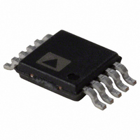
AD7687BRMZ Analog Devices Inc, AD7687BRMZ Datasheet - Page 17

AD7687BRMZ
Manufacturer Part Number
AD7687BRMZ
Description
IC ADC 16BIT 250KSPS 10-MSOP
Manufacturer
Analog Devices Inc
Series
PulSAR®r
Datasheet
1.AD7687BCPZRL7.pdf
(28 pages)
Specifications of AD7687BRMZ
Data Interface
DSP, MICROWIRE™, QSPI™, Serial, SPI™
Number Of Bits
16
Sampling Rate (per Second)
250k
Number Of Converters
1
Power Dissipation (max)
12.5mW
Voltage Supply Source
Single Supply
Operating Temperature
-40°C ~ 85°C
Mounting Type
Surface Mount
Package / Case
10-TFSOP (0.118", 3.00mm Width)
Resolution (bits)
16bit
Sampling Rate
250kSPS
Input Channel Type
Differential
Supply Voltage Range - Analog
2.3V To 5.5V
Supply Voltage Range - Digital
1.8V To 5.5V
Lead Free Status / RoHS Status
Lead free / RoHS Compliant
For Use With
EVAL-AD7687CBZ - BOARD EVALUATION FOR AD7687
Lead Free Status / RoHS Status
Lead free / RoHS Compliant, Lead free / RoHS Compliant
Available stocks
Company
Part Number
Manufacturer
Quantity
Price
Company:
Part Number:
AD7687BRMZ
Manufacturer:
ADI
Quantity:
1 000
Part Number:
AD7687BRMZ
Manufacturer:
ADI/亚德诺
Quantity:
20 000
Part Number:
AD7687BRMZ-REEL
Manufacturer:
ADI/亚德诺
Quantity:
20 000
Part Number:
AD7687BRMZ-RL7
Manufacturer:
ADI/亚德诺
Quantity:
20 000
Company:
Part Number:
AD7687BRMZRL7
Manufacturer:
ADI
Quantity:
1 000
Part Number:
AD7687BRMZRL7
Manufacturer:
ADI/亚德诺
Quantity:
20 000
range, as shown in Figure 32, which represents PSRR over
frequency.
The AD7687 powers down automatically at the end of each
conversion phase and, therefore, the power scales linearly with
the sampling rate, as shown in Figure 33. This makes the part
ideal for low sampling rate (even a few Hz) and low battery-
powered applications.
SUPPLYING THE ADC FROM THE REFERENCE
For simplified applications, the AD7687, with its low operating
current, can be supplied directly using the reference circuit
shown in Figure 34. The reference line can be driven by either:
•
•
•
insensitive to power supply variations over a wide frequency
0.001
1000
100
The system power supply directly
A reference voltage with enough current output capability,
such as the ADR43x
A reference buffer, such as the AD8031, which can also
filter the system power supply, as shown in Figure 34
0.1
95
90
85
80
75
70
65
60
55
50
10
10
1
VDD = 2.5V
VDD = 5V
Figure 33. Operating Currents vs. Sampling Rate
100
Figure 32. PSRR vs. Frequency
10
SAMPLING RATE (SPS)
FREQUENCY (kHz)
1000
100
VDD = 5V
10000
VIO
1000
100000
VDD = 2.5V
1000000
10000
Rev. A | Page 17 of 28
DIGITAL INTERFACE
Though the AD7687 has a reduced number of pins, it offers
flexibility in its serial interface modes.
The AD7687, when in CS mode, is compatible with SPI, QSPI,
digital hosts, and DSPs, for example, Blackfin® ADSP-BF53x or
ADSP-219x. This interface can use either 3-wire or 4-wire. A 3-
wire interface using the CNV, SCK, and SDO signals minimizes
wiring connections useful, for instance, in isolated applications.
A 4-wire interface using the SDI, CNV, SCK, and SDO signals
allows CNV, which initiates the conversions, to be independent
of the readback timing (SDI). This is useful in low jitter
sampling or simultaneous sampling applications.
The AD7687, when in chain mode, provides a daisy chain
feature using the SDI input for cascading multiple ADCs on a
single data line similar to a shift register.
The mode in which the part operates depends on the SDI level
when the CNV rising edge occurs. The CS mode is selected if
SDI is high and the chain mode is selected if SDI is low. The
SDI hold time is such that when SDI and CNV are connected
together, the chain mode is always selected.
In either mode, the AD7687 offers the flexibility to optionally
force a start bit in front of the data bits. This start bit can be
used as a BUSY signal indicator to interrupt the digital host and
trigger the data reading. Otherwise, without a BUSY indicator,
the user must time out the maximum conversion time prior to
readback.
The BUSY indicator feature is enabled as:
• In the CS mode, if CNV or SDI is low when the ADC
• In the chain mode, if SCK is high during the CNV rising edge
1
5V
OPTIONAL REFERENCE BUFFER AND FILTER.
conversion ends (
(Figure 46).
10kΩ
1μF
Figure 34. Example of Application Circuit
5V
AD8031
Figure 38
1
10μF
and
5V
Figure 42
REF
10Ω
).
AD7687
VDD
AD7687
1μF
VIO


