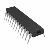
AD7730BN Analog Devices Inc, AD7730BN Datasheet - Page 46

AD7730BN
Manufacturer Part Number
AD7730BN
Description
IC ADC TRANSDUCER BRIDGE 24-DIP
Manufacturer
Analog Devices Inc
Datasheet
1.AD7730LBRUZ.pdf
(52 pages)
Specifications of AD7730BN
Mounting Type
Through Hole
Package / Case
24-DIP (0.300", 7.62mm)
Rohs Status
RoHS non-compliant
Number Of Bits
24
Sampling Rate (per Second)
1.2k
Data Interface
DSP, Serial, SPI™
Number Of Converters
1
Power Dissipation (max)
125mW
Voltage Supply Source
Analog and Digital
Operating Temperature
-40°C ~ 85°C
Peak Reflow Compatible (260 C)
No
No. Of Bits
24 Bit
Leaded Process Compatible
No
Features
Bridge Transducer ADC
No. Of Channels
2
Interface Type
Serial
For Use With
EVAL-AD7730LEBZ - BOARD EVALUATION FOR AD7730EVAL-AD7730EBZ - BOARD EVAL FOR AD7730
Lead Free Status / RoHS Status
Contains lead / RoHS non-compliant
Available stocks
Company
Part Number
Manufacturer
Quantity
Price
Company:
Part Number:
AD7730BN
Manufacturer:
ADI
Quantity:
9 002
AD7730/AD7730L
Parameter
LOGIC INPUTS
LOGIC OUTPUTS (Including MCLK OUT)
TRANSDUCER BURNOUT
OFFSET (TARE) DAC
SYSTEM CALIBRATION
POWER REQUIREMENTS
Input Current
All Inputs Except SCLK and MCLK IN
SCLK Only (Schmitt Trigerred Input)
MCLK IN Only
V
V
V
V
Floating State Leakage Current
Floating State Output Capacitance
AIN1(+) Current
AIN1(–) Current
Initial Tolerance @ 25 C
Drift
Resolution
LSB Size
DAC Drift
DAC Drift vs. Time
Differential Linearity
Positive Full-Scale Calibration Limit
Negative Full-Scale Calibration Limit
Offset Calibration Limit
Input Span
Power Supply Voltages
Power Supply Currents
Power Dissipation
OL
OL
OH
OH
V
V
V
V
V
V
V
V
V
V
V
V
V
AV
DV
AV
AV
DV
DV
AV
Normal Mode
Standby Mode
, Output Low Voltage
, Output Low Voltage
, Output High Voltage
, Output High Voltage
INL
INL
INH
T+
T+
T–
T–
T+
T+
INL
INL
INH
INH
2
DD
DD
DD
DD
DD
DD
DD
, Input Low Voltage
, Input Low Voltage
– V
– V
, Input Low Voltage
, Input Low Voltage
, Input High Voltage
, Input High Voltage
, Input High Voltage
– AGND Voltage
Current (Normal Mode)
Current (Normal Mode)
+ DV
Voltage
Current (Normal Mode)
Current (Normal Mode)
T–
T–
16
17
DD
Current (Standby Mode)
4, 16
18
2
17
17
B Version
0.8
0.4
2.0
1.4/3
1/2.5
0.8/1.4
0.4/1.1
0.4/0.8
0.4/0.8
0.8
0.4
3.5
2.5
0.4
0.4
4.0
V
9
–100
100
0.1
6
2.3/2.6
3.5
25
–0.25/+0.75
1.05
–1.05
–1.05
0.8
2.1
+4.75 to +5.25
+2.7 to +5.25
3.7
5.5
0.45
1
21
23.5
32.5
105
10
DD
10
10
– 0.6 V
FS
FS
FS
FS
FS
1
Units
V max
V max
V min
V min to V max
V min to V max
V min to V max
V min to V max
V min to V max
V min to V max
V max
V max
V min
V min
V max
V max
V min
V min
pF typ
nA nom
nA nom
% typ
%/ C typ
Bit
mV min/mV max
ppm/ C max
ppm/1000 Hours typ
LSB max
V max
V max
V max
V min
V max
V min to V max
V min to V max
mA max
mA max
mA max
mA max
mW max
mW max
A max
A max
A max
W max
–46–
Conditions/Comments
DV
DV
DV
DV
DV
DV
DV
DV
DV
DV
DV
DV
I
V
I
V
I
V
I
V
2.5 mV Nominal with 5 V Reference (REF IN/2000)
Guaranteed Monotonic
FS Is the Nominal Full-Scale Voltage
(10 mV, 20 mV, 40 mV or 80 mV)
With AGND = 0 V
External MCLK. Digital I/Ps = 0 V or DV
All Input Ranges Except 0 mV to +10 mV and 10 mV,
Typically 2.7 mA
Input Ranges of 0 mV to +10 mV and 10 mV Only,
Typically 4 mA
DV
DV
Typically 13 A. External MCLK IN = 0 V or DV
AV
All Input Ranges Except 0 mV to +10 mV and 10 mV,
Typically 15 mW
Input Ranges of 0 mV to +10 mV and 10 mV Only,
Typically 23.75 mW
Typically 65 W. External MCLK IN = 0 V or DV
SINK
SINK
SOURCE
SOURCE
DD
DD
DD
DD
DD
DD
DD
DD
DD
DD
DD
DD
DD
DD
DD
DD
DD
DD
DD
15
15
15
15
= 800 A Except for MCLK OUT
= 100 A Except for MCLK OUT
= DV
= +5 V
= +3 V
= +5 V
= +3 V
= +5 V
= +3 V
= +5 V
= +3 V
= +5 V
= +3 V
= +5 V
= +3 V
= +5 V
= +3 V
= +5 V
= +3 V
of 2.7 V to 3.3 V, Typically 0.3 mA
of 4.75 V to 5.25 V, Typically 0.75 mA
= 200 A Except for MCLK OUT
= 100 A Except for MCLK OUT
DD
= +5 V. Digital I/Ps = 0 V or DV
14
14
;
;
DD
14
14
;
;
DD
REV. A
DD
DD


