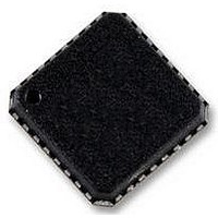
AD9649BCPZ-40 Analog Devices Inc, AD9649BCPZ-40 Datasheet - Page 10

AD9649BCPZ-40
Manufacturer Part Number
AD9649BCPZ-40
Description
IC ADC 14BIT 40MSPS 32LFCSP
Manufacturer
Analog Devices Inc
Datasheet
1.AD9649BCPZRL7-20.pdf
(32 pages)
Specifications of AD9649BCPZ-40
Data Interface
Serial, SPI™
Number Of Bits
14
Sampling Rate (per Second)
40M
Number Of Converters
1
Power Dissipation (max)
65.8mW
Voltage Supply Source
Analog and Digital
Operating Temperature
-40°C ~ 85°C
Mounting Type
Surface Mount
Package / Case
32-VFQFN, CSP Exposed Pad
Resolution (bits)
14bit
Sampling Rate
40MSPS
Input Channel Type
Differential
Supply Voltage Range - Analog
1.7V To 1.9V
Supply Voltage Range - Digital
1.7V To 3.6V
Lead Free Status / RoHS Status
Lead free / RoHS Compliant
Available stocks
Company
Part Number
Manufacturer
Quantity
Price
Company:
Part Number:
AD9649BCPZ-40
Manufacturer:
AD
Quantity:
6 700
AD9649
PIN CONFIGURATION AND FUNCTION DESCRIPTIONS
Table 8. Pin Function Descriptions
Pin No.
0 (EP)
1, 2
3, 24, 29, 32
4
5
6
7 to 12, 14 to 21
13
22
23
25
26
27
28
30, 31
Mnemonic
GND
CLK+, CLK−
AVDD
CSB
SCLK/DFS
SDIO/PDWN
D0 (LSB) to
D13 (MSB)
DRVDD
DCO
MODE/OR
VREF
SENSE
VCM
RBIAS
VIN−, VIN+
Description
Exposed Paddle. The exposed paddle is the only ground connection. It must be soldered to the analog
ground of the customer’s PCB to ensure proper functionality and maximize the heat dissipation, noise,
and mechanical strength benefits.
Differential Encode Clock for PECL, LVDS, or 1.8 V CMOS Inputs.
1.8 V Supply Pin for the ADC CORE Domain.
SPI Chip Select. Active low enable, 30 kΩ internal pull-up.
SPI Clock Input in SPI Mode (SCLK). 30 kΩ internal pull-down.
Data Format Select in Non-SPI Mode (DFS). Static control of data output format. 30 kΩ internal pull-down.
DFS high = twos complement output; DFS low = offset binary output.
SPI Data Input/Output (SDIO). Bidirectional SPI data I/O with 30 kΩ internal pull-down.
Non-SPI Mode Power-Down (PDWN). Static control of chip power-down with 30 kΩ internal pull-down.
See Table 14 for details.
ADC Digital Outputs.
1.8 V to 3.3 V Supply Pin for Output Driver Domain.
Data Clock Digital Output.
Chip Mode Select Input in SPI Mode (MODE).
Out-of-Range Digital Output in SPI Mode or in Non-SPI Mode (OR).
Default = out-of-range (OR) digital output (SPI Register 0x2A, Bit 0 = 1).
Option = chip mode select input (SPI Register 0x2A, Bit 0 = 0).
Chip power-down (SPI Register 0x08, Bits[7:5] = 100).
Chip stand-by (SPI Register 0x08, Bits[7:5] = 101).
Normal operation, output disabled (SPI Register 0x08, Bits[7:5] = 110).
Normal operation, output enabled (SPI Register 0x08, Bits[7:5] = 111).
In non-SPI mode, the pin operates only as an out-of-range (OR) digital output.
1.0 V Voltage Reference Input/Output. See Table 10.
Reference Mode Selection. See Table 10.
Analog Output Voltage at Mid AVDD Supply. Sets common mode of the analog inputs.
Set Analog Current Bias. Connect to 10 kΩ (1% tolerance) resistor to ground.
ADC Analog Inputs.
SDIO/PDWN
NOTES
1. THE EXPOSED PADDLE MUST BE SOLDERED TO THE ANALOG GROUND
SCLK/DFS
PLANE OF THE PCB TO ENSURE PROPER FUNCTIONALITY AND MAXIMIZE
THE HEAT DISSIPATION, NOISE, AND MECHANICAL STRENGTH BENEFITS.
D0 (LSB)
AVDD
CLK+
CLK–
CSB
D1
1
2
3
4
5
6
7
8
(Not to Scale)
PIN 1
INDICATOR
TOP VIEW
AD9649
Figure 3. Pin Configuration
Rev. 0 | Page 10 of 32
24 AVDD
23 MODE/OR
22 DCO
21 D13 (MSB)
20 D12
19 D11
18 D10
17 D9


