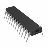
AD7710ANZ Analog Devices Inc, AD7710ANZ Datasheet - Page 26

AD7710ANZ
Manufacturer Part Number
AD7710ANZ
Description
IC ADC SIGNAL CONDITIONING 24DIP
Manufacturer
Analog Devices Inc
Datasheet
1.AD7710ARZ-REEL.pdf
(32 pages)
Specifications of AD7710ANZ
Data Interface
Serial
Number Of Bits
24
Sampling Rate (per Second)
1.03k
Number Of Converters
1
Power Dissipation (max)
45mW
Voltage Supply Source
Analog and Digital, Dual ±
Operating Temperature
-40°C ~ 85°C
Mounting Type
Through Hole
Package / Case
24-DIP (0.300", 7.62mm)
Resolution (bits)
24bit
Sampling Rate
1.02kSPS
Input Channel Type
Single Ended
Supply Voltage Range - Digital
4.75V To 5.25V
Supply Current
4.5mA
Digital Ic Case Style
DIP
Lead Free Status / RoHS Status
Lead free / RoHS Compliant
Available stocks
Company
Part Number
Manufacturer
Quantity
Price
Part Number:
AD7710ANZ
Manufacturer:
ADI/亚德诺
Quantity:
20 000
AD7710
MOV SCON,#00000000B;
MOV IE,#10010000B;
MOV IP,#00010000B;
SETB 91H;
SETB 90H;
MOV R1,#003H;
MOV R0,#030H;
MOV A,#00H;
MOV SBUF,A;
WAIT:
JMP WAIT;
INT ROUTINE:
NOP;
MOV A,R1;
JZ FIN;
DEC R1;
MOV A,@R;
INC R0;
RLC A;
MOV B.0,C; RLC A; MOV B.1,C; RLC A;
MOV B.2,C; RLC A; MOV B.3,C; RLC A;
MOV B.4,C; RLC A; MOV B.5,C; RLC A;
MOV B.6,C; RLC A: MOV B.7,C; MOV A,B;
CLR 93H;
CLR 91H;
MOV SBUF,A;
RETI;
FIN:
SETB 91H;
SETB 93H;
RETI;
Table VIII. 8XC51 Code for Writing to the AD7710
Configure 8051 for MODE 0
Operation and Enable Serial Reception
Enable Transmit Interrupt
Prioritize the Transmit Interrupt
Bring TFS High
Bring TFS High
Sets Number of Bytes to Be Written
in a Write Operation
Start Address in RAM for Bytes
Clear Accumulator
Initialize the Serial Port
Wait for Interrupt
Interrupt Subroutine
Load R1 to Accumulator
If Zero Jump to FIN
Decrement R1 Byte Counter
Move Byte into the Accumulator
Increment Address
Rearrange Data from LSB First
to MSB First
Bring A0 Low
Bring TFS Low
Write to Serial Port
Return from Subroutine
Set TFS High
Set A0 High
Return from Interrupt Subroutine
–26–
AD7710 to 68HC11 Interface
Figure 18 shows an interface between the AD7710 and the
68HC11 microcontroller. The AD7710 is configured for its
external clocking mode, while the SPI port is used on the 68HC11
in single-chip mode. The DRDY line from the AD7710 is con-
nected to the Port PC2 input of the 68HC11, so the DRDY line
is polled by the 68HC11. The DRDY line can be connected to
the IRQ input of the 68HC11 if an interrupt driven system is
preferred. The 68HC11 MOSI and MISO lines should be
configured for wire-OR operation. Depending on the interface
configuration, it may be necessary to provide bidirectional buff-
ers between the 68HC11 MOSI and MISO lines.
The 68HC11 is configured in master mode with its CPOL bit
set to a Logic 0 and its CPHA bit set to a logic 1. With a 10-MHz
master clock on the AD7710, the interface operates with all four
serial clock rates of the 68HC11.
68HC11
Figure 18. AD7710 to 68HC11 Interface
MISO
MOSI
SCK
PC2
PC0
PC3
PC1
SS
DV
DD
DV
DD
SYNC
RFS
TFS
DRDY
A0
SCLK
SDATA
MODE
AD7710
REV. G


