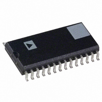
AD7863BR-3 Analog Devices Inc, AD7863BR-3 Datasheet - Page 17

AD7863BR-3
Manufacturer Part Number
AD7863BR-3
Description
IC ADC 14BIT DUAL 2CH 28-SOIC
Manufacturer
Analog Devices Inc
Datasheet
1.AD7863ARZ-3.pdf
(24 pages)
Specifications of AD7863BR-3
Rohs Status
RoHS non-compliant
Number Of Bits
14
Sampling Rate (per Second)
175k
Data Interface
Parallel
Number Of Converters
2
Power Dissipation (max)
94.5mW
Voltage Supply Source
Analog and Digital
Operating Temperature
-40°C ~ 85°C
Mounting Type
Surface Mount
Package / Case
28-SOIC (0.300", 7.50mm Width)
MICROPROCESSOR INTERFACING
The AD7863 high speed bus timing allows direct interfacing to
DSP processors as well as modern 16-bit microprocessors.
Suitable microprocessor interfaces are shown in Figure 19
through Figure 23.
AD7863 TO ADSP-2100 INTERFACE
Figure 19 shows an interface between the AD7863 and the
ADSP-2100. The CONVST signal can be supplied from the
ADSP-2100 or from an external source. The AD7863 BUSY line
provides an interrupt to the ADSP-2100 when conversion is
completed on both channels. The two conversion results can
then be read from the AD7863 using two successive reads to the
same memory address. The following instruction reads one of
the two results:
where:
MR0 is the ADSP-2100 MR0 register.
ADC is the AD7863 address.
AD7863 TO ADSP-2101/ADSP-2102 INTERFACE
The interface outlined in Figure 19 also forms the basis for an
interface between the AD7863 and the ADSP-2101/ADSP-2102.
The READ line of the ADSP-2101/ADSP-2102 is labeled RD . In
this interface, the RD pulse width of the processor can be
programmed using the data memory wait state control register.
The instruction used to read one of the two results is as outlined
for the ADSP-2100.
ADSP-2100
(ADSP-2101/
ADSP-2102)
MR0 = DM (ADC)
DMRD (RD)
DMA13
DMD15
DMA0
DMD0
IRQn
DMS
Figure 19. AD7863 to ADSP-2100 Interface
*ADDITIONAL PINS OMITTED FOR CLARITY.
EN
ADDRESS BUS
DATA BUS
DECODE
ADDR
CS
A0
BUSY
RD
DB13
DB0
OPTIONAL
AD7863*
CONVST
Rev. B | Page 17 of 24
AD7863 TO TMS32010 INTERFACE
An interface between the AD7863 and the TMS32010 is shown
in Figure 20. Once again the CONVST signal can be supplied
from the TMS32010 or from an external source, and the
TMS32010 is interrupted when both conversions have been
completed. The following instruction is used to read the
conversion results from the AD7863:
where:
D is data memory address.
ADC is the AD7863 address.
AD7863 TO TMS320C25 INTERFACE
Figure 21 shows an interface between the AD7863 and the
TMS320C25. As with the two previous interfaces, conversion
can be initiated from the TMS320C25 or from an external
source, and the processor is interrupted when the conversion
sequence is completed. The TMS320C25 does not have a
separate RD output to drive the AD7863 RD input directly. This
has to be generated from the processor STRB and R/ W outputs
with the addition of some logic gates. The RD signal is OR
gated with the MSC signal to provide the one WAIT state
required in the read cycle for correct interface timing.
Conversion results are read from the AD7863 using the
following instruction:
where:
D is data memory address.
ADC is the AD7863 address.
IN D, ADC
IN D, ADC
TMS32010
MEN
DEN
PA2
PA0
D15
Figure 20. AD7863 to TMS32010 Interface
INT
D0
*ADDITIONAL PINS OMITTED FOR CLARITY.
EN
ADDRESS BUS
DATA BUS
ADDRESS
DECODE
CS
A0
BUSY
RD
DB13
DB0
OPTIONAL
AD7863*
CONVST
AD7863


