AD7870SQ Analog Devices Inc, AD7870SQ Datasheet - Page 8
AD7870SQ
Manufacturer Part Number
AD7870SQ
Description
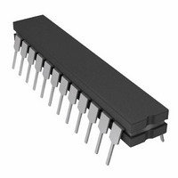
IC ADC 12BIT SAMPLING 3V 24-CDIP
Manufacturer
Analog Devices Inc
Datasheet
1.AD7870JNZ.pdf
(28 pages)
Specifications of AD7870SQ
Rohs Status
RoHS non-compliant
Number Of Bits
12
Sampling Rate (per Second)
100k
Data Interface
Serial, Parallel
Number Of Converters
1
Power Dissipation (max)
95mW
Voltage Supply Source
Dual ±
Operating Temperature
-55°C ~ 125°C
Mounting Type
Through Hole
Package / Case
24-CDIP (0.300", 7.62mm)
Available stocks
Company
Part Number
Manufacturer
Quantity
Price
Company:

Part Number:
AD7870SQ/883B
Manufacturer:
NEC
Quantity:
41


AD7870/AD7875/AD7876
PIN CONFIGURATIONS AND FUNCTION DESCRIPTIONS
Table 5. Pin Function Descriptions
DIP and SOIC
Pin No.
N/A
1
2
3
4
5
6
7
8 to11
12
13 to 16
17
DB10/SSTRB
DB11/HBEN
DB8/SDATA
PLCC
Pin No.
1, 8, 15,
22
2
3
4
5
6
7
9
10 to 13
14
16 to 19
20
Figure 2. DIP and SOIC Pin Configuration
DB9/SCLK
BUSY/INT
DB7/LOW
DB6/LOW
DB5/LOW
DB4/LOW
DGND
CLK
RD
10
12
11
1
2
3
4
5
6
7
8
9
Mnemonic
NC
RD
BUSY/INT
CLK
DB11/HBEN
DB10/SSTRB
DB9/SCLK
DB8/SDATA
DB7/LOW–
DB4/LOW
DGND
DB0/DB8
V
DB3/DB11–
DD
(Not to Scale)
AD7870/
AD7875/
AD7876
TOP VIEW
24
23
22
20
19
18
17
16
15
14
13
21
CS
CONVST
12/8/CLK
V
V
REF OUT
AGND
V
DB0/DB8
DB1/DB9
DB2/DB10
DB3/DB11
Function
No Connect.
Read. Active low logic input. This input is used in conjunction with CS low to enable the data outputs.
Busy/Interrupt. Active low logic output indicating converter status. See Figure 14, Figure 15, Figure 16,
and Figure 17.
Clock Input. An external TTL-compatible clock may be applied to this input pin. Alternatively, tying this
pin to V
Data Bit 11 (MSB)/High Byte Enable. The function of this pin is dependent on the state of the 12/8/CLK
input. When 12-bit parallel data is selected, this pin provides the DB11 output. When byte data is
selected, this pin becomes the HBEN logic input. HBEN is used for 8-bit bus interfacing. When HBEN is
low, DB7/LOW to DB0/DB8 become DB7 to DB0. With HBEN high, DB7/LOW to DB0/DB8 are used for
the upper byte of data (see
Data Bit 10/Serial Strobe. When 12-bit parallel data is selected, this pin provides the DB10 output.
SSTRB is an active low open-drain output that provides a strobe or framing pulse for serial data. An
external 4.7 kΩ pull-up resistor is required on SSTRB.
Data Bit 9/Serial Clock. When 12-bit parallel data is selected, this pin provides the DB9 output. SCLK is
the gated serial clock output derived from the internal or external ADC clock. If the 12/8/CLK input is at
−5 V, then SCLK runs continuously. If 12/8/CLK is at 0 V, then SCLK is gated off after serial transmission is
complete. SCLK is an open-drain output and requires an external 2 kΩ pull-up resistor.
Data Bit 8/Serial Data. When 12-bit parallel data is selected, this pin provides the DB8 output. SDATA is
an open-drain serial data output which is used with SCLK and SSTRB for serial data transfer. Serial data
is valid on the falling edge of SCLK while SSTRB is low. An external 4.7 kΩ pull-up resistor is required on
SDATA.
Three-state data outputs controlled by CS and RD. Their function depends on the 12/8/CLK and HBEN
inputs. With 12/8/CLK high, they are always DB7–DB4. With 12/8/CLK low or −5 V, their function is
controlled by HBEN (see
Digital Ground. Ground reference for digital circuitry.
Three-state data outputs which are controlled by CS and RD. Their function depends on the 12/8/CLK
and HBEN inputs. With 12/8/CLK high, they are always DB3–DB0. With 12/8/CLK low or −5 V, their
function is controlled by HBEN (see
Positive Supply, +5 V ± 5%.
SS
IN
DD
SS
enables the internal laser-trimmed clock oscillator.
Rev. C | Page 8 of 28
Table 6
Table 6
).
).
Table 6
).
DB10/SSTRB
DB11/HBEN
DB8/SDATA
DB9/SCLK
DB7/LOW
DB6/LOW
NC
Figure 3. PLCC Pin Configuration
10
11
5
6
7
8
9
INDENTFIER
12
4
AD7870/AD7875/
NC = NO CONNECT
13 14
3
(Not to Scale)
AD7876
TOP VIEW
PIN 1
2
15
1
16 17
28
27 26
18
25
24
23
22
21
20
19
V
V
REF OUT
NC
AGND
V
DB0/DB8
SS
IN
DD
Related parts for AD7870SQ
Image
Part Number
Description
Manufacturer
Datasheet
Request
R

Part Number:
Description:
±1.7g Dual-Axis IMEMS Accelerometer Evaluation Board
Manufacturer:
Analog Devices Inc
Datasheet:

Part Number:
Description:
Inertial Sensor Evaluation System
Manufacturer:
Analog Devices Inc
Datasheet:
Part Number:
Description:
Manufacturer:
Analog Devices Inc
Datasheet:
Part Number:
Description:
Manufacturer:
Analog Devices Inc
Datasheet:
Part Number:
Description:
Manufacturer:
Analog Devices Inc
Datasheet:
Part Number:
Description:
Manufacturer:
Analog Devices Inc
Datasheet:
Part Number:
Description:
Manufacturer:
Analog Devices Inc
Datasheet:
Part Number:
Description:
Manufacturer:
Analog Devices Inc
Datasheet:
Part Number:
Description:
Manufacturer:
Analog Devices Inc
Datasheet:
Part Number:
Description:
Manufacturer:
Analog Devices Inc
Datasheet:
Part Number:
Description:
Manufacturer:
Analog Devices Inc
Datasheet:
Part Number:
Description:
Manufacturer:
Analog Devices Inc
Datasheet:
Part Number:
Description:
Manufacturer:
Analog Devices Inc
Datasheet: