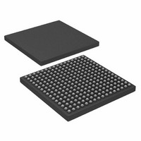
AD6654CBC Analog Devices Inc, AD6654CBC Datasheet - Page 27

AD6654CBC
Manufacturer Part Number
AD6654CBC
Description
IC ADC 14BIT W/4CH RSP 256CSPBGA
Manufacturer
Analog Devices Inc
Datasheet
1.AD6654CBCZ.pdf
(88 pages)
Specifications of AD6654CBC
Number Of Bits
14
Sampling Rate (per Second)
92.16M
Data Interface
Serial, Parallel
Number Of Converters
1
Power Dissipation (max)
2.5W
Voltage Supply Source
Analog and Digital
Operating Temperature
-25°C ~ 85°C
Mounting Type
Surface Mount
Package / Case
256-CSPBGA
Pin Count
256
Screening Level
Commercial
Package Type
CSPBGA
Lead Free Status / RoHS Status
Contains lead / RoHS non-compliant
Available stocks
Company
Part Number
Manufacturer
Quantity
Price
Company:
Part Number:
AD6654CBC
Manufacturer:
ADI
Quantity:
283
Company:
Part Number:
AD6654CBC
Manufacturer:
Analog Devices Inc
Quantity:
10 000
Part Number:
AD6654CBC
Manufacturer:
ADI/亚德诺
Quantity:
20 000
Company:
Part Number:
AD6654CBCZ
Manufacturer:
Analog Devices Inc
Quantity:
10 000
Part Number:
AD6654CBCZ
Manufacturer:
ADI/亚德诺
Quantity:
20 000
THEORY OF OPERATION
ADC ARCHITECTURE
The AD6654 analog-to-digital converter (ADC) front end
employs a 3-stage subrange architecture. This design approach
achieves the required accuracy and speed, while maintaining
low power consumption.
The AD6654 front end has complementary analog input pins,
AIN+ and AIN−, as shown in Figure 1. Each analog input is
centered at 2.4 V and should swing ±0.55 V around this
reference (see Figure 36). Because AIN+ and AIN− are 180°
out of phase, the differential full-scale analog input signal is
2.2 V p-p.
Both analog inputs are buffered prior to the first track-and-
hold, TH1. The high state of the ENCODE pulse places TH1 in
hold mode. The held value of TH1 is applied to the input of a
5-bit coarse ADC1. The digital output of ADC1 drives a 5-bit
digital-to-analog converter, DAC1. DAC1 requires 14 bits of
precision that is achieved through laser trimming.
Rev. 0 | Page 27 of 88
The output of DAC1 is subtracted from the delayed analog
signal at the input of TH3 to generate a first residue signal. TH2
provides an analog pipeline delay to compensate for the digital
delay of ADC1.
The first residue signal is applied to a second conversion stage
consisting of a 5-bit ADC2, 5-bit DAC2, and pipeline TH4. The
second DAC requires 10 bits of precision, which is met by the
process with no trim. The input to TH5 is a second residue
signal generated by subtracting the quantized output of DAC2
from the first residue signal held by TH4. TH5 drives a final
6-bit ADC3.
The digital outputs from ADC1, ADC2, and ADC3 are added
together and corrected in the digital error correction logic to
generate the final output data. The latency of the ADC core is
four CLK cycles. The resulting 14-bit ADC data is internally
routed directly to the integrated DDC for processing by the
4/6 independent DDC channels.
AD6654


