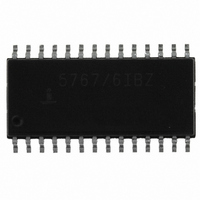
HI5767/6IBZ Intersil, HI5767/6IBZ Datasheet - Page 7

HI5767/6IBZ
Manufacturer Part Number
HI5767/6IBZ
Description
CONV A/D 10BIT 60MSPS 28-SOIC
Manufacturer
Intersil
Datasheet
1.HI57672CBZ.pdf
(15 pages)
Specifications of HI5767/6IBZ
Number Of Bits
10
Sampling Rate (per Second)
60M
Data Interface
Parallel
Number Of Converters
8
Power Dissipation (max)
310mW
Voltage Supply Source
Analog and Digital
Operating Temperature
-40°C ~ 85°C
Mounting Type
Surface Mount
Package / Case
28-SOIC (0.300", 7.50mm Width)
Lead Free Status / RoHS Status
Lead free / RoHS Compliant
Electrical Specifications
NOTES:
Maximum Output Current
DIGITAL INPUTS
Input Logic High Voltage, V
Input Logic Low Voltage, V
Input Logic High Current, I
Input Logic Low Current, I
Input Capacitance, C
DIGITAL OUTPUTS
Output Logic High Voltage, V
Output Logic Low Voltage, V
Output Three-State Leakage Current, I
Output Logic High Voltage, V
Output Logic Low Voltage, V
Output Three-State Leakage Current, I
Output Capacitance, C
TIMING CHARACTERISTICS
Aperture Delay, t
Aperture Jitter, t
Data Output Hold, t
Data Output Delay, t
Data Output Enable Time, t
Data Output Enable Time, t
Data Latency, t
Power-Up Initialization
Sample Clock Pulse Width (Low)
Sample Clock Pulse Width (High)
Sample Clock Duty Cycle Variation
POWER SUPPLY CHARACTERISTICS
Analog Supply Voltage, AV
Digital Supply Voltage, DV
Digital Output Supply Voltage, DV
Supply Current, I
Power Dissipation
Offset Error Sensitivity, ∆V
Gain Error Sensitivity, ∆FSE
2. Parameter guaranteed by design or characterization and not production tested.
3. With the clock low and DC input.
LAT
AJ
AP
CC
PARAMETER
H
OD
IN
OUT
IL
IH
CC1
OS
IL
CC
IH
EN
DIS
OL
OL
OH
OH
7
CC2
AV
C
Unless Otherwise Specified (Continued)
L
CC
= 10pF; T
OZ
OZ
= DV
CC1
A
= 25
= 5.0V, DV
CLK, DFS, OE
CLK, DFS, OE
CLK, DFS, OE, V
CLK, DFS, OE, V
I
I
V
I
I
V
For a Valid Sample (Note 2)
Data Invalid Time (Note 2)
f
f
f
At 3.0V
At 5.0V
f
f
AV
AV
OH
OL
OH
OL
S
S
S
IN
IN
o
O
O
C; Differential Analog Input; Typical Values are Test Results at 25
= 40MSPS
= 40MSPS
= 40MSPS
CC
CC
= 1MHz and DFS = “0”
= 1MHz and DFS = “0”
= 0/5V; DV
= 0/5V; DV
= 100µA; DV
= 100µA; DV
= 100µA; DV
= 100µA; DV
or DV
or DV
CC2
TEST CONDITIONS
CC
CC
HI5767
= 3.0V; V
CC2
CC2
= 5V ±5%
= 5V ±5%
CC2
CC2
CC2
CC2
IH
IL
= 5V
= 3V
= 0V
= 5V
= 5V
= 3V
= 5V
= 3V
REFIN
= V
REFOUT
; f
S
= 40MSPS at 50% Duty Cycle;
-10.0
-10.0
11.3
11.3
4.75
4.75
4.75
MIN
2.0
4.0
-10
2.4
-10
2.7
-
-
-
-
-
-
-
-
-
-
-
-
-
-
-
-
-
-
-
± 0.7
± 0.1
TYP
12.5
12.5
310
5.0
5.0
3.0
5.0
10
± 5
62
±1
±1
7
5
5
5
6
5
5
-
-
-
-
-
-
-
-
-
-
-
o
+10.0
+10.0
C,
MAX
5.25
5.25
5.25
0.2
0.8
0.8
0.5
3.3
10
10
20
7
-
-
-
-
-
-
-
-
-
-
-
-
-
-
-
-
-
-
UNITS
ps
Cycles
Cycles
LSB
LSB
mW
mA
mA
µA
µA
µA
µA
pF
pF
ns
RMS
ns
ns
ns
ns
ns
ns
%
V
V
V
V
V
V
V
V
V
V


